Become a MacRumors Supporter for $50/year with no ads, ability to filter front page stories, and private forums.

B S Magnet

macrumors 601
Original poster
Hi. Longtime, but occasional reader here.

So I've owned a couple of Rev. C clamshells (an indigo and a 466 key lime) over the last dozen years.

With the latter, I restored it partially earlier this year — adding a 128GB SSD, a DVD-RW (which mates to the original bezel), and an LG XGA 1024x768 LCD (using shifuimam's fantastic sleuthing back in 2007 on another long gone forum), with its anti-glare sheet removed (yet another hack found elsewhere). The modem card was also removed for a future project. In all, it's lighter, quicker, and more versatile than Apple ever intended for it.

I'm throwing this to the brave souls (@LightBulbFun, @dosdude1, and others) who've successfully made the G4 chip swap on PPC750L (Rev. A & B) clamshells, namely because they've likely had more close-up face time with the clamshell logic board than most folks.

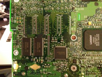
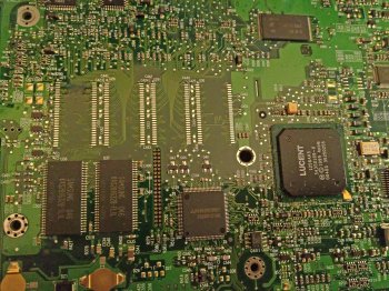
On the overside and underside of the northbridge logic board (with Rev. C logic boards), one can make out the locations on either of the board side where onboard memory modules are soldered (providing 64MB of onboard memory for Rev. C, and 32 MB for Rev. A & B).

On the underside of the Rev. C (and ostensibly on the underside of Revs. A & B), there's an additional area adjacent to the underside soldered memory where space allocations for four more memory modules appeared to be planned for a future use, but ultimately were not (as the ice dual-USB iBooks were rushed to production).

The number of PCB contact pads would suggest 4 additional memory modules of the same type, with pads for the same kind of transistors between modules, bringing a hypothetical "Rev. D" board to 128MB onboard (or higher, in theory, if using higher-density memory sourced from a 512MB SO-DIMM, at 64MB per module).

IMG_20181205_151857a.jpg


In any event, I've searched fairly extensively for documentation for these unused spots on the logic board — in particular, to suss whether anyone comfortable with micro-soldering has ever attempted to solder memory modules (donated from an SO-DIMM) to produce a higher onboard memory baseline… and succeeded.

As there aren't any close-ups of this area on the logic board anywhere online, I'm adding them here (one above, two more attached). The photos are of my dead indigo's board (now a parts donor for the key lime).

Handing this to you all: what do you know about these?
 

Attachments

  • IMG_20181205_151631a.jpg
    IMG_20181205_151631a.jpg
    2.2 MB · Views: 367
  • IMG_20181205_151926a.jpg
    IMG_20181205_151926a.jpg
    3 MB · Views: 336
  • Like
Reactions: AphoticD

AphoticD

macrumors 68020
Feb 17, 2017
2,283
3,465
@LightBulbFun had discussed the idea of replacing the onboard modules with higher capacity ones, but I don’t think there was success as there may have been a limitation within the memory controller not addressing above the stock config.

I’m sure he could expand upon this if he is about. :)
 

B S Magnet

macrumors 601
Original poster
@LightBulbFun had discussed the idea of replacing the onboard modules with higher capacity ones, but I don’t think there was success as there may have been a limitation within the memory controller not addressing above the stock config.

I’m sure he could expand upon this if he is about. :)

Thanks. Hopefully will hear back from folks on this. My hypothesis is they were intended for modules at the same density as the other soldered modules (16mb), yielding a potential onboard total of 128mb + the added 512mb.

Of course, I was also fathoming the fantastical notion that the onboard modules (both pre-existing and the open spots being discussed in this thread) could be bumped up to the 64mb density, yielding an incomprehensible onboard total of 512mb, pushing this to a 1gb machine.

But one step at a time.
 

0248294

Cancelled
Jan 10, 2016
713
869
I wouldn't be too surprised if that would work, if all the traces from those pads are connected to the appropriate components on the board and the memory controller can address more than the physical maximum memory on these machines, and if there are no software limitations. An example of this is the original Xbox, the consumer versions (other than the final version 1.6 release), had empty RAM pads. On developer kits and the SEGA Chihiro arcade system (which is based on the Xbox logic board), these pads would be occupied by a further 64MB of RAM, totalling it to 128MB vs the 64MB on consumer models. It did require software hacking as the consumer software wouldn't address it, and only mostly homebrew software like emulators took advantage of it, but it was certainly doable. Also, its CPU could be upgraded to a faster Pentium III, much like how the Clamshell's G3 can be upgraded to a 7410 G4 processor, which has been done before.
 

weckart

macrumors 603
Nov 7, 2004
5,900
3,582
Might be worth a look to see if there are any limitations set by the hardware checks in the Clamshell firmware. It would be a shame to have cracked the soldering to falter to a reboot loop or failing POST altogether.
 
  • Like
Reactions: AphoticD

LightBulbFun

macrumors 68030
Nov 17, 2013
2,892
3,189
London UK
@LightBulbFun had discussed the idea of replacing the onboard modules with higher capacity ones, but I don’t think there was success as there may have been a limitation within the memory controller not addressing above the stock config.

I’m sure he could expand upon this if he is about. :)

sadly i never got a chance to try swapping in some more RAM sticks (the G4 iBook G3 did not survive an attempted L2 cache swap/upgrade, well the machine POSTed but the L2 would not be recognised so I reused the G4 elsewhere, I suspect that was because of my soldering, those TSOP chips are a right B*tch)

as mentioned in total theres 8 Memory Chip pads allowing for a theoretical maximum of 512MB onboard+512MB in the SODIMM slot for 1GB total

but what I dont know is how the onboard memory is detected via OpenFirmware, without schematics its hard to tell if onboard memory amount is set by some sort of hardware strap or not, I do know the first clamshells where 32MB onboard then upgraded to 64MB onboard but still with 4 chips only

the first thing to do would of course be adding 4 more chips of the same type already on the motherboard and see if that works, and then move onto replacing all the chips with higher density versions, (its also worth mentioning you would also have to populate all the passives like the bypass capacitors next to the RAM chips)
 

B S Magnet

macrumors 601
Original poster
Aw. Darn. I would have loved to hear how that went.

I didn't know the 32MB boards used four modules (at 8MB each?).

The first thing I would need to do before adding 4 more chips of the same type is to have a spare logic board on hand in case I ruin the main one, a much better soldering iron, flux, (at least I have a good wick ribbon), and much better soldering skills.

It isn't to say I won't one day do these. In fact, my ultimate hope/plan/goal is to verify that the four pads for memory modules actually function without major OF alterations, swap the PPC750CX chip with the 700MHz chip from the summer 2001 iMac, integrating a USB hub card in place of the modem I removed previously, and swapping the CCF and backlight inverter with an LED retrofit. I'm also building another battery since finding good replacements is becoming challenging.

But first, I should probably get an OK soldering iron and practise.

sadly i never got a chance to try swapping in some more RAM sticks (the G4 iBook G3 did not survive an attempted L2 cache swap/upgrade, well the machine POSTed but the L2 would not be recognised so I reused the G4 elsewhere, I suspect that was because of my soldering, those TSOP chips are a right B*tch)

as mentioned in total theres 8 Memory Chip pads allowing for a theoretical maximum of 512MB onboard+512MB in the SODIMM slot for 1GB total

but what I dont know is how the onboard memory is detected via OpenFirmware, without schematics its hard to tell if onboard memory amount is set by some sort of hardware strap or not, I do know the first clamshells where 32MB onboard then upgraded to 64MB onboard but still with 4 chips only

the first thing to do would of course be adding 4 more chips of the same type already on the motherboard and see if that works, and then move onto replacing all the chips with higher density versions, (its also worth mentioning you would also have to populate all the passives like the bypass capacitors next to the RAM chips)
 

0248294

Cancelled
Jan 10, 2016
713
869
A 700MHz Clamshell would be pretty crazy, although you probably would want to beef the cooling up a bit to accomodate for the higher TDP. DIY batteries shouldn't be too hard, 8 Bit Guy even has a video where he does this, although he used pretty crappy cells, and soldered them instead of spot welding, which is not recommended as soldering the batteries generates more heat and could cause cells, especially cruddy ones, to burn up. And battery cell fires ain't fun.
 

B S Magnet

macrumors 601
Original poster
A 700MHz Clamshell would be pretty crazy, although you probably would want to beef the cooling up a bit to accomodate for the higher TDP. DIY batteries shouldn't be too hard, 8 Bit Guy even has a video where he does this, although he used pretty crappy cells, and soldered them instead of spot welding, which is not recommended as soldering the batteries generates more heat and could cause cells, especially cruddy ones, to burn up. And battery cell fires ain't fun.

Yah I've seen that how-to on YT before, and will be relying on it as carefully as I can for the battery rebuild. I've ordered the LG HG2 series batteries, which I understand are quite good at high-drain situations.

As for cooling, I re-seated the heatsink and other chip pads (all of which were oily goo) with a very good heat-transfer paste, and I leave istat running for at least the thermometer on the SSD (in absence of a sensor for the chip).

For a 700MHz plan, I haven't yet arrived to an effective heat dissipation method in the absence of a fan, but in all the years I've run the 466, I've never truly reached what felt like a hot chip the way, say, a G5 or Intel chip often do.

One other thing I haven't figured out since adding the XGA monitor is how to get ATIccelerator to recognize that the machine is still running with an ATI Rage Mobility 128 onboard. For now, the system lacks any video overclocking I once had.

Anyway, here are some shots of its present state.
IMG_20180609_211821.jpg
IMG_20180608_172419_edit_1528493146225.jpg
 

B S Magnet

macrumors 601
Original poster
That matching led light in green...great detail!

Love it!

Total fluke. I found it at the hardware store earlier this year for, like, $4, and it was close enough a match to make it worthwhile, even if i rarely actually use it.

Oh. Presently, it takes 38 seconds to boot to the login screen. I hope to trim a couple of seconds from that.
 
  • Like
Reactions: Traace

B S Magnet

macrumors 601
Original poster
but what I dont know is how the onboard memory is detected via OpenFirmware, without schematics its hard to tell if onboard memory amount is set by some sort of hardware strap or not, I do know the first clamshells where 32MB onboard then upgraded to 64MB onboard but still with 4 chips only

So fwiw, I have located a source for schematics on the Rev C. clamshell, although it appears the only way to access the file itself is to first enrol in a not-inexpensive course. I doubt they're going to willingly just make this available to anyone who asks nicely.

Until anything further, this find amounts to close only counting in horseshoes, hand grenades, h-bombs, and habañero peppers.
 
Register on MacRumors! This sidebar will go away, and you'll see fewer ads.