Become a MacRumors Supporter for $50/year with no ads, ability to filter front page stories, and private forums.

name99

macrumors 68020
Jun 21, 2004
2,407
2,309
I think you misunderstand what Philip is doing. He tested both AMX and the GPU. His work on the GPU side is both to evaluate its feasibility for double-precision calculation as well as explore possibilities for porting CUDA code.
Fair enough. In these sorts of threads we are all working with (sometimes very) imperfect information :-(
I wish there were somewhere I could see a writeup of his work on the AMX side (and for that matter of what his issues are on the Metal side).

Certainly it seems there is massive scope (IMHO) for more sophisticated utilization of the multiple throughput engines we have available! I've mentioned things like random number generation, but one also suspects that interesting things are possible (more complex, of course, but possible) for various relaxation algorithms, to run a round at fp16, then a round at fp32, then a round at fp64, and repeat. Of course games like this now have to pay a cost in terms of reformatting data; but that's an easy add-on to both GPU and AMX if there's value to having it.
 

Philip Turner

macrumors regular
Dec 7, 2021
170
111
  • Like
Reactions: name99 and jdb8167

name99

macrumors 68020
Jun 21, 2004
2,407
2,309
Most likely, IMHO, due to revenues from STEM are not consistent and/or attractive eough for Apple.
I suspect it's even simpler than that. Jobs was friends with Richard Crandall and Steven Wolfram (I guess he met both through NeXT) and was willing to support them and give them visible Apple support (effectively media oxygen) on the basis of his interests and beliefs.
But Crandall of course died ten years ago, and Tim Cook seems to have a different set of interests (not worse, just different). So people like Ali Sazegari are doing interesting work within Apple, but he and his team don't get media oxygen the way Crandall did.

We in STEM are used to being ignored and in the background! It's not that Apple doesn't care about our use cases (or our dollars); it's just that we will buy regardless and don't much need to be fed a story, whereas the video type uses cases (including eg drawing, or music creation or whatever) are a space where Apple feels they can acquire new customers, either from professionals moving downward ("work on plane") or amateurs moving upward ("hey teens, did you know you can make your own movie, even with special effects?").
 
  • Like
Reactions: richmlow

name99

macrumors 68020
Jun 21, 2004
2,407
2,309
Can third parties use Apple's AMX? Is it still undocumented?
Undocumented by Apple, yes.
There is a fair amount of documentation by others. I explain the basic capabilities and how they have evolved in my PDFs
https://github.com/name99-org/AArch64-Explore (look at vol 3 for the AMX section, which is around page 180), and I reference others, like Dougall, who give the actual opcodes.

On your personal Mac, you could probably write AMX assembly without constraints and my GUESS is that Apple would not (unlike for the iPhone store) prevent the distribution of such code (ie scan it when it's first copied onto the drive and mark it as "illegal execution"). But of course writing assembly is something of a minority pursuit!
If you control the compiler (like Julia) you have more flexibility! I think it would be a fascinating exercise for someone on the Julia team to make a side version that routes directly to AMX to see what the results are – if interesting enough, we may be able to get Apple to lighten up on the AMX policy (which remember, began in the world of iPhone, which is a rather different world). If someone wants to do this, REALLY start by reading my AMX stuff, to get a feel for what is there today, how much has changed in each iteration, and why I state that it is heading towards being something like Apple's version of AVX-512.

For now the ideal would be to have all the various BLAS/LAPACK/EIGEN type libraries make use of Apple's Accelerate calls which route to AMX (and similarly for eg FFT); but there are always impedance matches between how one body of code has been doing things and how Apple has set up its APIs :-(
 
  • Like
Reactions: Andropov

name99

macrumors 68020
Jun 21, 2004
2,407
2,309
I recently benchmarked Accelerate vs. OpenBLAS. For most operations, Accelerate is faster because it uses AMX. But for complex eigendecomposition (needed for quantum chemistry), OpenBLAS is 2x faster. The number of FLOPS is also so low, that you wouldn't need AMX. At least for the non-complex eigendecomposition, Apple gets >50 FP64 GFLOPS while on single-core. That says they're using AMX but not parallelizing. OpenBLAS gets slightly better performance with multithreading.

For complex eigendecomposition, you have to un-interleave data before feeding to the AMX. This might not prevent reaching maximum FLOPS for ZGEMM, but requires more threads. Accelerate uses 4 threads for DGEMM (haven't checked ZGEMM), but doesn't multithread its AMX in ZHEEVD. Again, this may not be problematic. Apple gets 34 GFLOPS using one core, OpenBLAS gets 68 GFLOPS using 2-4 cores. DFT simulations can perform multiple eigendecompositions in parallel so you might call into Accelerate ZGEMM from 8 threads. OpenBLAS might do 2-4 eigendecompositions in parallel, therefore slower overall. I haven't benchmarked that yet.

[Data Attached]

For SGEMM and DGEMM, calling into Accelerate from multiple threads wrecked performance. If it's the same with eigendecomposition, I could get better performance using the GPU. If it doesn't (meaning CPU achieves ~300 GFLOPS), even emulated double-single won't provide much speedup (<550 GFLOPS). Mind quantum chemistry does 100% of calculation in FP64, MD is a different story.


I've seen mentions on MATLAB forums that you can direct it to a different BLAS library. In that case, you can change OpenBLAS to Accelerate.
Apologies if you know this but plenty of people still do not, and it might help you both understand your results and optimize future code.

AMX is a PER-CLUSTER resource, not a PER-CPU resource. Think of AMX as attached to the L2 of a cluster. This has multiple consequences.
- There is one AMX unit for the P-cluster [ie 4 P-cores] and one (less hardware, so some operations are performed by iterating them) for the E-cluster. A Pro or Max have two P-AMX units and one E-AMX unit.
- Data to the AMX unit "preferentially" comes from L2, if it's in L1 there will be a few extra cycles to transport it out to L2/AMX.

- So naively
you will not get any sort of AMX boost by using multiple threads on an M1/M2;
you will if you use two threads on a Pro/Max (AND those threads are dispatched to separate clusters, but the OS scheduler seems OK in this regard).

- BUT this naive view is far from accurate for various reasons, each of which may or may not be relevant
+ the AMX unit replicates registers for all four client cores, and can execute code from each core simultaneously, or interleaved across cycles
+ time will be required to move data from a core to L2/AMX, and while this is happening AMX execution can happen on behalf of another core
+ POSSIBLY using the E-AMX will provide some boost (if your work doesn't require frequent synchronizations between threads; but it may provide a horrible slowdown if the P-AMX frequently has to wait for the E-AMX [running at perhaps a third of the speed of the P-AMX once you take HW resources and frequency into account]

- Beyond the above, in patents (and it is unclear how far the patents are running ahead of implementation, or what the differences are between M1 and M2) we see improvements along the following lines
+ packing two AMX instructions into a single transaction from the CPU core to AMX
+ better AMX support for multiple simultaneous transactions (eg load/store simultaneously with an outer product)
+ support for vector-vector operations (eg component-wise multiply or add)
+ support for two such independent vector-vector operations per cycle

- And of course Accelerate keeps improving their code base.

You mentioned that M2 Pro/Max have doubled the number of AMX resources. I have not heard that and don't know how you learned it, but what you may be seeing is simply the implementation of some of the above ideas (which are REALLY nice, in that for the cost of a few percent extra hardware you get close to performance doubling across almost all use cases!)

So summary of all this is ultimately one has to keep trying and seeing what works on each new device. But
- for the AMX eigen stuff, do you have two P-clusters? ie do you expect to be able to usefully run AMX on two threads? Perhaps Accelerate believes that your calls max out the single AMX unit? (Or perhaps Accelerate just hasn't yet got around to anything beyond basic optimization?)
- for SGEMM and DGEMM, were you perhaps using so many threads that you were pushing the OS to use the E-AMX? In which case, as I described, possible nasty synchronization slow-downs! Before bothering to try to fix this in code, you could probably detect it just by looking at CPU utilization in Performance Monitor.
 

Xiao_Xi

macrumors 68000
Oct 27, 2021
1,627
1,101
AMX is a PER-CLUSTER resource, not a PER-CPU resource. Think of AMX as attached to the L2 of a cluster. This has multiple consequences.
- There is one AMX unit for the P-cluster [ie 4 P-cores] and one (less hardware, so some operations are performed by iterating them) for the E-cluster. A Pro or Max have two P-AMX units and one E-AMX unit.
- Data to the AMX unit "preferentially" comes from L2, if it's in L1 there will be a few extra cycles to transport it out to L2/AMX.
69502024-a55e-4ceb-bbd4-0cf1193153d8_1024x421.jpg

 
Last edited:

name99

macrumors 68020
Jun 21, 2004
2,407
2,309
I'm not doing much on the AMX side - pretty much exclusively GPU.

Extensive documentation of the M1 GPU microarchitecture (complements Dougall Johnson's): https://github.com/philipturner/metal-benchmarks

Drafting an FP64 emulation library: https://github.com/philipturner/metal-float64

Metal backend for hipSYCL: https://github.com/illuhad/hipSYCL/issues/864
Thanks so much for those.
The Metal FP64 stuff is beautiful work, and I'm now reading the GPU design stuff. It's so nice to find someone with the same sort of interests as me, in terms of trying to figure out exactly how a microarchitecture works, and how it has evolved over time.
 

Philip Turner

macrumors regular
Dec 7, 2021
170
111
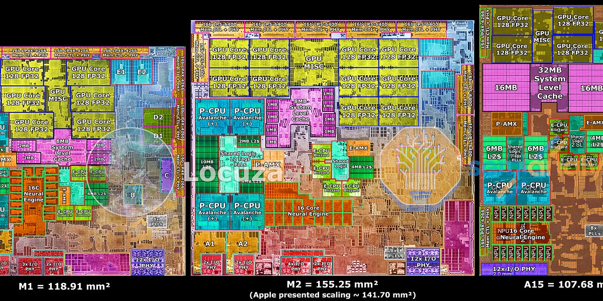
You mentioned that M2 Pro/Max have doubled the number of AMX resources. I have not heard that and don't know how you learned it, but what you may be seeing is simply the implementation of some of the above ideas
Apple_M1-Pro-M1-Max_M1-Pro_10182021.jpg

Apple-M2-chips-M2-Pro-230117.jpg

Minimalist E-cores still have 2 blocks, that's all one thread can typically utilize.
 
Last edited:

Philip Turner

macrumors regular
Dec 7, 2021
170
111
for SGEMM and DGEMM, were you perhaps using so many threads that you were pushing the OS to use the E-AMX?
If you call two Swift threads pushing the OS to its limits. I was searching for the fastest way to multiply matrices, and it was always a single-threaded call into Accelerate. You can try for yourself and verify this: source code. I remember seeing 200% in the activity monitor, although in something recent (I cannot remember where) I saw 400% utilized.
 

Philip Turner

macrumors regular
Dec 7, 2021
170
111
the AMX unit replicates registers for all four client cores
I forgot that, but remember there's individual AMX blocks. Each takes 4 cycles performing one 512-bit by 512-bit multiplication. It cannot perform multiple multiplications simultaneously, that would violate my model of FLOPS. Same with ANE, which actually has slightly higher clock speed than the GPU. The recent jump from 11 -> 15.8 TFLOPS coincided with something larger on the die. If I attribute that to just clock speed, they'd jump 1.4 GHz to 2.0 GHz in a single generation. Not likely - especially since M2 Pro ANE looks so different from M1 Pro ANE. Rather, I think their cores now either (1) perform two multiplications simultaneously taking 6 cycles or (2) perform one in 3 cycles - not sure that's physically possible.

ChipDate ReleasedTSMCGPU MHzANE MHzANE OPs/Core
A11Sep/22/2017N10106611701024?/4 Cycles
A12/A12XSep/21/2018N7112812202048/4 Cycles
A13Sep/20/2019N7P123013402048/4 Cycles
A14/M1Oct/23/2020N5127813402048/4 Cycles
M1 ProOct/26/2021N5129613402048/4 Cycles
A15Sep/24/2021N5P133814504096/6? Cycles
M2/M2 ProJun/24/2022N5P139814504096/6? Cycles
A16Sep/7/2022N4139815604096/6? Cycles
Assuming ANE also operates on 512-bit operands, cores would be slightly smaller than AMX because less complex circuitry (no FP64, not even multiple data types). The size gap seems to have closed with A15/M2 (Pro), leading to the idea that it does more in parallel, not higher clock.

Back to AMX cores : CPUs assignment, I was explaining the amount of physical hardware actually used. One CPU core cannot issue enough instructions to satisfy 4 blocks, and overheads you mentioned limit that to 2 blocks in most use cases. The ISA might say all registers are mapped, but I doubt AMX would shuffle registers between blocks at will (costing extra clock cycles). Probably you're supposed to pin certain registers to each CPU, or else face unexpected astronomical switching latencies.

For example, you perform a 512-bit by 512-bit outer product. Now kilobytes of data are stored in one AMX block. Next instruction, you want to multiply-accumulate another outer product to those same kilobytes. I imagine the AMX would perform said instruction inside the same AMX block. If a CPU only dispatches an AMX multiply every 4 cycles, it might automatically pin one block to one CPU, to reduce data movement. How accurate is this idea?
 
Last edited:

Philip Turner

macrumors regular
Dec 7, 2021
170
111
Is it me, or does it look like the M2 Pro was designed by using artificial intelligence (what Nvidia did with Hopper)? The GPU L2 cache and media encoders look less square, like not how a human would design something.

Perhaps we should make a website, which annotates each pixels in each die shot. It would be an interactive experience to try explaining what each square mm of the chip is. For example, a register for a GPU core, some L1 memory for an ANE core, some interconnect circuitry to route memory requests. It would also let us discover cache sizes for things like media encoders, or how an SLC block operates.
 
Last edited:

name99

macrumors 68020
Jun 21, 2004
2,407
2,309
View attachment 2144914
View attachment 2144915
Minimalist E-cores still have 2 blocks, that's all one thread can typically utilize.
I've seen these sorts of photos floating around. What I haven't seen is reliable explanations of what the marked up regions are supposed to represent. For all we know, the apparently increased area (if it's even dedicated to AMX, which is not clear) may be there for energy saving purposes rather than performance purposes.

If Apple had simple duplicated the AMX resources available (two AMX blocks per P-cluster) I think that would have been part of the video! Whereas the sorts of tweaks I described, being much more difficult and technical to explain, they would not have mentioned.
 

name99

macrumors 68020
Jun 21, 2004
2,407
2,309
If you call two Swift threads pushing the OS to its limits. I was searching for the fastest way to multiply matrices, and it was always a single-threaded call into Accelerate. You can try for yourself and verify this: source code. I remember seeing 200% in the activity monitor, although in something recent (I cannot remember where) I saw 400% utilized.
You stated
"
For SGEMM and DGEMM, calling into Accelerate from multiple threads wrecked performance. If it's the same with eigendecomposition, I could get better performance using the GPU. If it doesn't (meaning CPU achieves ~300 GFLOPS), even emulated double-single won't provide much speedup (<550 GFLOPS). Mind quantum chemistry does 100% of calculation in FP64, MD is a different story.
"
but you didn't provide details of what counts as "multiple threads" or whether you were using a machine with 2 P-clusters. If you were using a machine with a single P-cluster, then I'm guessing the second thread is routed to the E-cluster AMX, with the issues I describe.

I'm not trying to fight you here; I'm trying to explain what the issues are for people who want to get the most out of the hardware, because my experience has been that people simply have no clue exactly what AMX is – the very idea of a piece of hardware that is shared at the cluster level, rather than being dedicated to a core, is something they'd never thought of. (Though Apple does it quite a bit. There is also an LZ-engine at the cluster level, used for page compression, and there's good reason to believe that the L2 TLB is shared at the cluster level.)


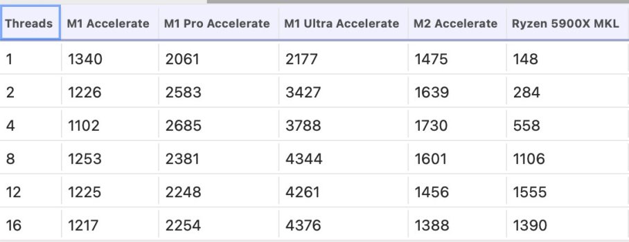
These results, for example, I think are most explicable in terms of what I have described:
(Obviously with all manner of caveats in terms of the matrix sizes and suchlike.)

gemm-benchmark:
FhIf_xkXkAALGYp.jpeg


The essential pattern (one M1 AMX unit gets you 1300, two get you 2600, four get you 5200) is essentially there.
For details my GUESS is that
- Accelerate on a Pro behind the scenes routes the instructions to both AMX units (ie creates its own internal extra thread) but doesn't do a perfect job of this (matrices too small? and cost of moving data between two clusters). So there is some amount of slack in AMX usage which is available for exploitation by a second thread.

- For the Ultra Accelerate doesn't even seem to be trying hard to use the second chiplet (which may be a SW optimization issue, or may reflect the fact that the coherence protocol across the two chiplets is not yet optimal; Ultra scaling is disappointing for many purposes. Apple have patented [and I discuss] a protocol and NoC that should improve this a lot, but it's unclear when they will ship (as it's unclear even when/if the M2 Ultra will ship).

- The M2 case does not show a 2x improvement, but it does show a nice 30% improvement (a lot better than you'd expect just from the 7% or so frequency improvement. I think this is because of the various tweaks I described that allow a lot more cases of simultaneous 2-wide execution in an AMX units, once multiple flows of independent instruction streams are being routed to AMX from different cores.
 

Attachments

  • FhIf_xkXkAALGYp.jpeg
    FhIf_xkXkAALGYp.jpeg
    45.6 KB · Views: 102

name99

macrumors 68020
Jun 21, 2004
2,407
2,309
I forgot that, but remember there's individual AMX blocks. Each takes 4 cycles performing one 512-bit by 512-bit multiplication. It cannot perform multiple multiplications simultaneously, that would violate my model of FLOPS. Same with ANE, which actually has slightly higher clock speed than the GPU. The recent jump from 11 -> 15.8 TFLOPS coincided with something larger on the die. If I attribute that to just clock speed, they'd jump 1.4 GHz to 2.0 GHz in a single generation. Not likely - especially since M2 Pro ANE looks so different from M1 Pro ANE. Rather, I think their cores now either (1) perform two multiplications simultaneously taking 6 cycles or (2) perform one in 3 cycles - not sure that's physically possible.

ChipDate ReleasedTSMCGPU MHzANE MHzANE OPs/Core
A11Sep/22/2017N10106611701024?/4 Cycles
A12/A12XSep/21/2018N7112812202048/4 Cycles
A13Sep/20/2019N7P123013402048/4 Cycles
A14/M1Oct/23/2020N5127813402048/4 Cycles
M1 ProOct/26/2021N5129613402048/4 Cycles
A15Sep/24/2021N5P133814504096/6? Cycles
M2/M2 ProJun/24/2022N5P139814504096/6? Cycles
A16Sep/7/2022N4139815604096/6? Cycles
Assuming ANE also operates on 512-bit operands, cores would be slightly smaller than AMX because less complex circuitry (no FP64, not even multiple data types). The size gap seems to have closed with A15/M2 (Pro), leading to the idea that it does more in parallel, not higher clock.

Back to AMX cores : CPUs assignment, I was explaining the amount of physical hardware actually used. One CPU core cannot issue enough instructions to satisfy 4 blocks, and overheads you mentioned limit that to 2 blocks in most use cases. The ISA might say all registers are mapped, but I doubt AMX would shuffle registers between blocks at will (costing extra clock cycles). Probably you're supposed to pin certain registers to each CPU, or else face unexpected astronomical switching latencies.

For example, you perform a 512-bit by 512-bit outer product. Now kilobytes of data are stored in one AMX block. Next instruction, you want to multiply-accumulate another outer product to those same kilobytes. I imagine the AMX would perform said instruction inside the same AMX block. If a CPU only dispatches an AMX multiply every 4 cycles, it might automatically pin one block to one CPU, to reduce data movement. How accurate is this idea?
I'm not sure what you mean by "AMX block" or this entire sentence: "I forgot that, but remember there's individual AMX blocks. Each takes 4 cycles performing one 512-bit by 512-bit multiplication. It cannot perform multiple multiplications simultaneously, that would violate my model of FLOPS."

Again, apologies if I am telling you what you already know, but do you understand what the AMX hardware looks like? How it is 8x8 "units" with each unit holding its own FMAC (which can perform 1 64x64 MAC, or two 32x32 MACs or 4 16x16 MACs) along with its own storage. corsix describes this to a small extent; I describe it in much more detail.
If your mental model is something like SIMD (or Intel's AMX) Apple's HW is very different, performing multiplication as a "1-D sum of outer products" rather than as a "2D sum of inner products".
Also in case you think there have to be four "blocks" for four cores, no! To put it simply each register is duplicated four times within the AMX hardware, so the X0 register has four versions, one for CPU 0, for CPU 1, 2, 3.
(Obviously the way you'd actually implement this is with a larger pool of registers and with per-client renaming...)

One thing that's very clever about the design (and not at all obvious) is that while the source registers (X and Y, as vectors) are treated like normal register file registers, the results in the Z "register" are in fact distributed storage, with the appropriate elements stored at each one of these 8x8 hardware units. So yes, there IS a large amount of output Z-storage involved (and replicated 4x, once for each client core!) but it's distributed in such a way that there aren't the physical scaling costs associated with accessing a single huge register file.

As for ANE, we have some idea of what the internals look like by looking at the patents. The master patent is here:
https://patents.google.com/patent/US20190340491A1
Look for other patents also, in the name of Liran Fishel.
Essentially (to my non-expert eyes) the patent trail looks like both the ISP and Display Engine were separately implementing convolution engines of some sort, and the common elements to both of these were extracted, beefed up, labeled the ANE, and made available more generally. I don't know nearly enough about this space to comment any further; but one thing that strikes me from the patents is that instruction control seems to operate at a much larger granularity than either AMX or a GPU. The low power (and area) are achieved by having few options, and very little optionality (ie allowing one subset to go down a different path from a different subset as in a GPU); it's all about one engine pulling in data, while a single instruction stream is applying a fairly hardwired data rearrangement, then MACs, then lookup, to different data.
 

name99

macrumors 68020
Jun 21, 2004
2,407
2,309
Is it me, or does it look like the M2 Pro was designed by using artificial intelligence (what Nvidia did with Hopper)? The GPU L2 cache and media encoders look less square, like not how a human would design something.

My guess is that you are correct. Apple seems to have extremely high quality design tools (rapid turnaround, easy retargeting of a design to a different foundry or different process, apparently few design errors) and I would guess that they're a lot more aware than you and I are of what can be done with AI in this space.

nV have also mentioned using AI to design cache replacement algorithms. What was presented in the slides did not strike me as very impressive, but I may not understand the problem space (GPU caching as opposed to CPU caching) and they may have been deliberately cagey about saying anything more than the basic "we threw AI at the problem and got surprisingly good improvements to our cache utilization".
One suspects Apple are engaged in the same sort of enterprise!
 

Philip Turner

macrumors regular
Dec 7, 2021
170
111
but you didn't provide details of what counts as "multiple threads" or whether you were using a machine with 2 P-clusters.
I have two different meanings of threads. One is, Accelerate fires up multiple CPU cores behind the scenes. That is multiple CPU cores within a single-threaded context. You don't need to use pthreads or Grand Central Dispatch to perform this multithreading.

Orthogonally, is the "smart" idea of performing multiple BLAS operations in parallel. Since my 8 AMX blocks (4 per P-cluster) are only being utilized to ~70%, perhaps oversaturate their instruction stream with two simultaneously SGEMM multiplications. Maybe ALU utilization will jump to ~90%. This is accomplished with some simple Swift code:

Swift:
import Foundation
import Accelerate

let numThreads = 2
let matricesA: [Matrix] = .init(repeating: .zeroes, count: numThreads)
let matricesB: [Matrix] = .init(repeating: .zeroes, count: numThreads)
let matricesC: [Matrix] = .init(repeating: .zeroes, count: numThreads)

let start = CACurrentMediaTime()
DispatchQueue.concurrentPerform(iterations: numThreads) { i in
    matricesC[i] = cblas_sgemm(matricesA[i], matricesB[i])
}
let end = CACurrentMediaTime()
let flops = computeFlops(start, end, matricesA[0].size)

Counterintuitively, ALU utilization did not improve! On the quoted image, this is actually the case with M1. Two parallel multiplications reduces F32-GFLOPS from 1300 to 1200 (of 1600 theoretical). With the benchmarked M1 Pro, how many iterations did they run, and what was the matrix size? I achieved 2746 GFLOPS from a 960x960 matrix multiply. It shot down drastically after exceeding the L2 cache, and larger matrices never exceeded 2056 GFLOPS.

For the Ultra Accelerate doesn't even seem to be trying hard to use the second chiplet
That is not true. The Ultra exceeds 3305 GFLOPS with just two parallel matrix multiplications. In that case, this requires a two-threaded context (let numThreads = 2). Communicating over UltraFusion has so much overhead, that a single-threaded context (let numThreads = 1) cannot efficiently harness AMX from both pairs of P-clusters. Or maybe I'm wrong. I hypothesize that matrices spanning several gigabytes (e.g. 40000x40000) would activate a 8 (4???)-P-core, 16-AMX-block fast-path inside Accelerate. Therefore 2x2056=4112 GFLOPS would be accessible from a single-threaded context (let numThreads = 1).

A note about benchmarks, try performing ~100 consecutive multiplies from the same thread, no wait between. That should boost the single-threaded and dual-threaded numbers closer to hardware maxima. A15 P-cores should reach similar GFLOPS to M1, M2 similar to M1 Pro, M2 Pro similar to M1 Ultra.
 

name99

macrumors 68020
Jun 21, 2004
2,407
2,309
I have two different meanings of threads. One is, Accelerate fires up multiple CPU cores behind the scenes. That is multiple CPU cores within a single-threaded context. You don't need to use pthreads or Grand Central Dispatch to perform this multithreading.

Orthogonally, is the "smart" idea of performing multiple BLAS operations in parallel. Since my 8 AMX blocks (4 per P-cluster) are only being utilized to ~70%, perhaps oversaturate their instruction stream with two simultaneously SGEMM multiplications. Maybe ALU utilization will jump to ~90%. This is accomplished with some simple Swift code:

Swift:
import Foundation
import Accelerate

let numThreads = 2
let matricesA: [Matrix] = .init(repeating: .zeroes, count: numThreads)
let matricesB: [Matrix] = .init(repeating: .zeroes, count: numThreads)
let matricesC: [Matrix] = .init(repeating: .zeroes, count: numThreads)

let start = CACurrentMediaTime()
DispatchQueue.concurrentPerform(iterations: numThreads) { i in
    matricesC[i] = cblas_sgemm(matricesA[i], matricesB[i])
}
let end = CACurrentMediaTime()
let flops = computeFlops(start, end, matricesA[0].size)

Counterintuitively, ALU utilization did not improve! On the quoted image, this is actually the case with M1. Two parallel multiplications reduces F32-GFLOPS from 1300 to 1200 (of 1600 theoretical). With the benchmarked M1 Pro, how many iterations did they run, and what was the matrix size? I achieved 2746 GFLOPS from a 960x960 matrix multiply. It shot down drastically after exceeding the L2 cache, and larger matrices never exceeded 2056 GFLOPS.


That is not true. The Ultra exceeds 3305 GFLOPS with just two parallel matrix multiplications. In that case, this requires a two-threaded context (let numThreads = 2). Communicating over UltraFusion has so much overhead, that a single-threaded context (let numThreads = 1) cannot efficiently harness AMX from both pairs of P-clusters. Or maybe I'm wrong. I hypothesize that matrices spanning several gigabytes (e.g. 40000x40000) would activate a 8 (4???)-P-core, 16-AMX-block fast-path inside Accelerate. Therefore 2x2056=4112 GFLOPS would be accessible from a single-threaded context (let numThreads = 1).

A note about benchmarks, try performing ~100 consecutive multiplies from the same thread, no wait between. That should boost the single-threaded and dual-threaded numbers closer to hardware maxima. A15 P-cores should reach similar GFLOPS to M1, M2 similar to M1 Pro, M2 Pro similar to M1 Ultra.
I can't comment on this because your mental model of AMX seems so at odds with reality. You seem constantly surprised by things that strike me as obvious IF one has the correct mental model of the HW.

I've tried to describe what's going on with AMX, with plenty of supporting data. That's all I can do.
 

Philip Turner

macrumors regular
Dec 7, 2021
170
111
I'm not sure what you mean by "AMX block" or this entire sentence:

Again, apologies if I am telling you what you already know, but do you understand what the AMX hardware looks like?
Apple_M1-Pro-M1-Max_M1-Pro_10182021.jpg


Half the M1 Pro's P-CPU can perform 1600 GFLOPS FP32. That is 500 FLOPs/cycle @ 3.2 GHz. FFMA takes 4 cycles to complete because of physics, so the entire hardware does 2000 FLOP's in 4 cycles. 2000 FLOP's is 1000 FMAs, so you multiplied 32 floats* with 32 floats to get 1024 floats. The entire unit, however, divided that into chunks. Each block contains 1/4 the compute power captured in the image above. Therefore one block cannot multiply all of the 32 floats (or perhaps it does, but takes 16 cycles to do so???).

* When I say floats, I mean 32-bit floats. You could fit 16 of these into a 512-bit register. A double is 64-bit, 8 fit into a 512-bit register. A half is 16-bit, 32 fit into a 512-bit register.

My interpretation, one block multiplies 16 floats or 8 doubles. That is 512 bits or 64 bytes, the same as an AMX register size. Apple can scale the number of AMX blocks to increase each AMX-cluster's compute power. The E-cores have two AMX blocks inside their cluster, and subsequently half the compute power (at equal clocks) as either P-cluster. M2 Pro AMX-clusters have 8 blocks, and subsequently twice the compute power as M1 Pro. Whether the ISA implements that by breaking up larger multiplications into 512-bit by 512-bit chunks, I do not consider.

I remember posting something on MacRumors. I found the theoretical number of transistors necessary to multiply two 16-bit integers. I used it to predict the size of an ANE "core" with striking accuracy. My mental model, AMX blocks and ANE cores are very similar. Each takes a 512-bit chunk of X, 512-bit chunk of Y, and multiplies them in 4 clock cycles. The ANE matrix multiplier variant would multiply 32 halfs x 32 halfs = 1024 half-precision multipliers. 9,000 transistors make up a 16-bit x 16-bit integer multiplier*. That resolves to 9,216,000 transistors per ANE core, or 147,456,000 transistors for the ALUs in the entire M1 neural engine. TSMC N5 has 138.2 million transistors per square millimeter. Therefore our lower bound is 1.067 mm^2.

*I'm treating 16-bit floats (half-precision) just like 16-bit ints. We actually have 11-bit multipliers creating 22-bit products, with extra circuit complexity to process exponents and add stuff. I say a simple 16-bit multiplier is a conservative estimate of transistor count.

Now, take the M1 die shot and look at the 16 things sticking out from the edges of the ANE's center. Narrow down your vision to the silvery part (which is compute), ignoring the brown stuff surrounding that. Those are ANE cores. Visually rearrange them into one contiguous chunk. What you get is smaller than a GPU core (3 mm^2). Perhaps this area is actually 2 mm^2. My conservative estimate (1.067 mm^2) is (a) lower and (b) quite close. That cannot be a coincidence. Let's recap.

----

I don't care how data is dispatched to a unit. Perhaps an AMX block or ANE core takes 1024 bits of data. Splits them into 512-bit chunks, takes 4 cycles to multiply each chunk, 16 cycles overall. Still the same amount of GFLOPS, same amount of transistors.

1) I have direct way to map GFLOPS/(4-)clock to number of transistors, and therefore area on the die. Unlike GPU and CPU, matrix multipliers are the most dense arithmetic circuitry physically possible. You can correlate GFLOPS to die area, perhaps within a factor of 2.

2) Based on performance benchmarks, the AMX does not have any special FP16-multiplying hardware. Please prove me wrong, and provide a test where my M1 Max CPU gets 6.6 TFLOPS FP16. FP32 and FP16 GFLOPS are the same. The assembly ISA might work with FP16 data types, but hardware ultimately decompresses them to FP32. Then it feeds them into 256 single-precision multipliers per block. They cost (from Wikipedia) ~21,000 transistors. Overall, that's 5,376,000 transistors per AMX block. Less than ANE, but there's a catch. These transistors can be repurposed into 64 double-precision multipliers. That's got to drive up transistor cost, plus the 64-bit mantissa adders and other overheads.

3) Finally, I assume one AMX block consumes more transistors than one ANE core. In theory it's ~5,376,000 vs ~9,000,000 but in reality probably ~20,000,000 vs ~18,000,000. Do the math and overlay the die area onto one of the M1-series die shots.
 
Last edited:

Philip Turner

macrumors regular
Dec 7, 2021
170
111
Okay, I guess the ANE core's silvery part and AMX block's silvery part are not that similar in size. Perhaps the AMX blocks* actually have 4x the number of transistors. Or, most of those transistors are stuff other than the 32x32-bit multipliers or 64x64-bit multipliers.

*In the M1 chip's P-cluster, the singular AMX-cluster contains 4 AMX-blocks. You can see these in the die shot.

Still, the math applies. Certain hardware is multipliers, part of a larger building block that takes 4 cycles to do FFMA. How many multipliers you have, directly defines the number of FLOPS. If clock speeds and measured FLOPS are correct, each rectangular box inside the AMX cluster contains 256 FP32 multipliers. Or you can reimagine them as performing the four 32-bit x 32-bit blocks of a 64-bit x 64-bit multiplication. Each 1/16 of the ANE must contain 1024 FP16 multipliers.
 
Last edited:

name99

macrumors 68020
Jun 21, 2004
2,407
2,309
View attachment 2144999

Half the M1 Pro's P-CPU can perform 1600 GFLOPS FP32. That is 500 FLOPs/cycle @ 3.2 GHz. FFMA takes 4 cycles to complete because of physics, so the entire hardware does 2000 FLOP's in 4 cycles. 2000 FLOP's is 1000 FMAs, so you multiplied 32 floats* with 32 floats to get 1024 floats. The entire unit, however, divided that into chunks. Each block contains 1/4 the compute power captured in the image above. Therefore one block cannot multiply all of the 32 floats (or perhaps it does, but takes 16 cycles to do so???).

* When I say floats, I mean 32-bit floats. You could fit 16 of these into a 512-bit register. A double is 64-bit, 8 fit into a 512-bit register. A half is 16-bit, 32 fit into a 512-bit register.

My interpretation, one block multiplies 16 floats or 8 doubles. That is 512 bits or 64 bytes, the same as an AMX register size. Apple can scale the number of AMX blocks to increase each AMX-cluster's compute power. The E-cores have two AMX blocks inside their cluster, and subsequently half the compute power (at equal clocks) as either P-cluster. M2 Pro AMX-clusters have 8 blocks, and subsequently twice the compute power as M1 Pro. Whether the ISA implements that by breaking up larger multiplications into 512-bit by 512-bit chunks, I do not consider.

I remember posting something on MacRumors. I found the theoretical number of transistors necessary to multiply two 16-bit integers. I used it to predict the size of an ANE "core" with striking accuracy. My mental model, AMX blocks and ANE cores are very similar. Each takes a 512-bit chunk of X, 512-bit chunk of Y, and multiplies them in 4 clock cycles. The ANE matrix multiplier variant would multiply 32 halfs x 32 halfs = 1024 half-precision multipliers. 9,000 transistors make up a 16-bit x 16-bit integer multiplier*. That resolves to 9,216,000 transistors per ANE core, or 147,456,000 transistors for the ALUs in the entire M1 neural engine. TSMC N5 has 138.2 million transistors per square millimeter. Therefore our lower bound is 1.067 mm^2.

*I'm treating 16-bit floats (half-precision) just like 16-bit ints. We actually have 11-bit multipliers creating 22-bit products, with extra circuit complexity to process exponents and add stuff. I say a simple 16-bit multiplier is a conservative estimate of transistor count.

Now, take the M1 die shot and look at the 16 things sticking out from the edges of the ANE's center. Narrow down your vision to the silvery part (which is compute), ignoring the brown stuff surrounding that. Those are ANE cores. Visually rearrange them into one contiguous chunk. What you get is smaller than a GPU core (3 mm^2). Perhaps this area is actually 2 mm^2. My conservative estimate (1.067 mm^2) is (a) lower and (b) quite close. That cannot be a coincidence. Let's recap.

----

I don't care how data is dispatched to a unit. Perhaps an AMX block or ANE core takes 1024 bits of data. Splits them into 512-bit chunks, takes 4 cycles to multiply each chunk, 16 cycles overall. Still the same amount of GFLOPS, same amount of transistors.

1) I have direct way to map GFLOPS/(4-)clock to number of transistors, and therefore area on the die. Unlike GPU and CPU, matrix multipliers are the most dense arithmetic circuitry physically possible. You can correlate GFLOPS to die area, perhaps within a factor of 2.

2) Based on performance benchmarks, the AMX does not have any special FP16-multiplying hardware. Please prove me wrong, and provide a test where my M1 Max CPU gets 6.6 TFLOPS FP16. FP32 and FP16 GFLOPS are the same. The assembly ISA might work with FP16 data types, but hardware ultimately decompresses them to FP32. Then it feeds them into 256 single-precision multipliers. They cost (from Wikipedia) ~21,000 transistors. Overall, that's 5,376,000 transistors per AMX block. Less than ANE, but there's a catch. These transistors can be repurposed into 64 double-precision multipliers. That's got to drive up transistor cost, plus the 64-bit mantissa adders and other overheads.

3) Finally, I assume one AMX block consumes more transistors than one ANE core. In theory it's ~5,376,000 vs ~9,000,000 but in reality probably ~20,000,000 vs ~18,000,000. Do the math and overlay the die area onto one of the M1-series die shots.

I'm sorry but that diagramming makes no sense to me. We know how the AMX unit works at a logical level (as I have described). How its laid out (even assuming the part assumed to be AMX actually is so...) is of secondary relevance.

We have 64 baseline units (in an 8x8 config). These are pipelined. Each can handle an FP64.
Hence we would expect that we can perform
64 (hardware) * 2 (FMAC) * 3.2 (approx GHz) = 422 GFlops.

That's indeed what we see:

For FP32 my memory was that the FP64 FMAC HW could be reconfigured to two FP32 FMAC's, but it seems like it's actually four. (This may have changed between AMX1 and 2; I forget the details with so much of this stuff and so many changes!)
Hence 4x the performance, 1.688 TFlops. This order of magnitude matches the twitter post I gave, with the obvious proviso that exact numbers depend on matrix size (and other details like how whether the source or dest data needs to move between L1 and L2).

For both cases, for large enough matrices we seem to go a little higher; my guess is that at some point Accelerate deems if worthwhile to also dispatch part of the calculation the the E-cluster's AMX.

I have no idea where your numbers come from; as I keep telling you, whatever your mental model is of AMX (perhaps based on GPU?) it does not seem to match the actual hardware. The hardware is not even a "matrix multiply unit" in the sense of how I think GPU Tensor Cores (and definitely Intel AMX) are "matrix multiply units"; it performs an OUTER product (plus local accumulate), not a matrix product, so the dataflow patterns are very different.

There are multiple other things that can be said (for example about FP16 and the integer cases) but I think that's all pointless until we get on the same page regarding what the AMX hardware actually IS (as far as the programming/performance model is concerned; I'm uninterested in how its laid out on the chip), and what it's limitations are.

The IMPORTANT points I am trying to make are
- one AMX unit per cluster
- Accelerate does an adequate (perhaps not fully optimized, or perhaps not fully exploited at smaller matrix sizes) job of using all the AMX units available, first the P-units and then, for large enough problems, the E-units. It appears to do a less than adequate job of using all the Ultra units, but that MAY reflect the fact that for the cases where we have numerical data (like the Twitter post) the matrices were not large enough.

- If a single problem does not 100% max out the AMX units, starting a second Accelerate "instance" (let's call that) dealing with a completely independent problem MAY get you closer to 100% performance. MAY being the operative word. If you were limited by non-compute overhead (like moving data around) then throwing more OF THE SAME TYPE of work at the problem will not help things, in the same way that you can't get more work out of a maxed out AVX512 unit if you switch to hyperthreading.

But improvements in M2 AMX have allowed for at least some of this overhead of moving instructions and data between the CPU and AMX, and within AMX, to be reduced (eg move twice as many instructions per cycle, overlap data movement with compute inside AMX, a larger degree of OoO reordered execution within AMX). We see this to some extent with a single Accelerate "instance" but we get more of a boost with multiple Accelerate "instances" because now the independent instructions are not all fighting with each other over things like access to the bus between each core and AMX (they can pack multiple instructions in a single transaction), and the OoO reordering has more flexibility when there is a larger pool of instructions that are not sequentially dependent.
 

Philip Turner

macrumors regular
Dec 7, 2021
170
111
it performs an OUTER product
I think of each rectangle inside the AMX as a grid. Let's keep it to FP64 for simplicity. The grid has 8 columns and 8 rows, with 64 units that will multiply stuff.

X0X1X2X3X4X5X6X7
Y0
Y1
Y2
Y3
Y4
Y5
Y6
Y7

Now, shoot the X data down through the entire grid. This only requires handling 8 doubles, or 64 B of data. Quite simple in hardware.

X0X1X2X3X4X5X6X7
Y0X0X1X2X3X4X5X6X7
Y1X0X1X2X3X4X5X6X7
Y2X0X1X2X3X4X5X6X7
Y3X0X1X2X3X4X5X6X7
Y4X0X1X2X3X4X5X6X7
Y5X0X1X2X3X4X5X6X7
Y6X0X1X2X3X4X5X6X7
Y7X0X1X2X3X4X5X6X7

Now do the same horizontally. You've scattered the Y values into the multipliers. The upper left contains X0 and Y0, the one right of that contains X1 and Y0, the next contains X2 and Y0, etc. Multiply!

Remember the layout of the pipeline in the Apple GPU ALU. There are 4 pipelines, and each cycle you dispatch an instruction to a separate one. You dispatch: 1st pipeline, 2nd pipeline, 3rd pipeline, 4th pipeline, 1st pipeline. By the time you looped back to the 1st pipeline, its FFMA has completed (it took 4 cycles). I think of the M1 P-AMX like this. One CPU is supposed to dispatch to the first of the 4 rectangles. Then dispatch to the second, third, fourth. Loop back around to the first. It's just like any other FFMA ALU setup, 4 pipelines with 4-cycle latency = 1-cycle throughput. You think that every cycle, the entire engine takes 64 B of X and Y and generates its outer product. In reality, it doesn't. Each block duplicates the circuitry for 64 B x 64 B multiplication.

On the E-cores, they have half the amount of transistors in the AMX-stuff. They also have half the amount of SIMD vector pipelines (8 128-bit @ 4 cycles). You can pretend they're 2 128-bit @ 1 cycle, an oversimplification. The SIMD and AMX are absolutely unrelated, and it's also a terrible analogy (think of E-AMX cluster like 1 512-bit X & Y @ 2 cycle throughput). One E-AMX rectangle is 1 512-bit X & Y @ 4 cycle.

SIMD PipelinesE-CoresP-Cores
Takes4 cycles4 cycles
Appears0.5 cycle (2 NEONs/clock)0.25 cycle (4 NEONs/clock)
Concurrency = Latency/Throughput8 pipelines16 pipelines
How many NEON ALUs?2 (2 NEONs/clock)4 (4 NEONs/clock)
Pipelines/ALU4 (8 pipelines/2 NEONs)4 (16 pipelines/4 NEONs)

Now think about the GPU. You've seen my reverse-engineering efforts. Each of the 128 scalar ALUs can have 4 floats in flight, simultaneously doing an FFMA. They might be at different stages, but the circuitry is duplicated. Well, maybe no. It's easiest to think that way, regardless of whether you actually have 512 multiplication circuits/core. Perhaps each separate pipeline takes turns accessing a common FP32 multiplier, takes turns accessing a mantissa adder, takes turns accessing other stuff. If that's true, I'm way off, and overestimated the number of hardware multipliers by a factor of 4.

Are we on the same page so far?
 
Last edited:

name99

macrumors 68020
Jun 21, 2004
2,407
2,309
" I think of the M1 P-AMX like this."
Well it isn't :)
I've tried to tell you this a dozen times. You can read my PDF's, or Dougall, or corsix, or the patents.
I think there is no point in further discussion until you are willing to read some of this material and accept that it behaves nothing like the GPU and your mental model.

Yes 8x8 grid.
Yes X values flow down and Y values flow across.
Then a SINGLE instruction executes which tells each of the 8x8 independent blocks to perform its operation from the data in its two registers and store the result locally.
Think of like a SIMD instruction that, instead of being 2x64b wide (for NEON) it's (8x8)x64b wide -- but ONE "SIMULTANEOUS" instruction...

I'm not trying to be rude here, just efficient. You have an incorrect mental model (justified! my initial mental model of AMX was very incorrect, as was Dougall's, and it took some thought and experiment by both of us to converge on reality, confirmed when I discovered the relevant patents).

I have to sleep now, but seriously, read some of what I have suggested, and then we can take this further.
 

leman

macrumors Core
Oct 14, 2008
19,517
19,664
@Philip Turner As the conversation now is about mental models (and I think it’s an important one), I wanted to add that I do not quite follow your use of the term “pipeline”. You seem to be regularly using it in context like “dispatch to different pipelines” etc. which to me implies that there are multiple compute units that augment each other to improve the throughput. But I always thought that pipelines are stages within one unit, and each pipeline is responsible for a part of an operation. As it is executed, an operation travels through the pipelines and is completed when it has passed through all the pipelines. At the same time, as an operation leaves a pipeline stage, another operation can enter the stage.

In other words, my mental model of pipelines is like a single rail track with multiple stations, and operations are like trains, which travel from station to another. This allows efficient hardware reuse and improves throughput, as it might take multiple stages (train stations) to execute an operation, but new trains are being dispatched all the time so that a station is never idling empty - there are multiple trains on the track which stop at different stations. Your description of pipelines instead seems to be multiple rail tracks (e.g. four for Apple GPU) with one train per track and most stations being empty.

Which mental model is correct?
 

Xiao_Xi

macrumors 68000
Oct 27, 2021
1,627
1,101
In other words, my mental model of pipelines is like a single rail track with multiple stations, and operations are like trains, which travel from station to another. This allows efficient hardware reuse and improves throughput, as it might take multiple stages (train stations) to execute an operation, but new trains are being dispatched all the time so that a station is never idling empty - there are multiple trains on the track which stop at different stations. Your description of pipelines instead seems to be multiple rail tracks (e.g. four for Apple GPU) with one train per track and most stations being empty.
Since people describe AMX as a coprocessor and not an accelerator like NPU, I mentally picture AMX as a very sophisticated shared execution unit just like any other execution unit that the CPU has like the floating point unit. Am I very wrong?
 

leman

macrumors Core
Oct 14, 2008
19,517
19,664
Since people describe AMX as a coprocessor and not an accelerator like NPU, I mentally picture AMX as a very sophisticated shared execution unit just like any other execution unit that the CPU has like the floating point unit. Am I very wrong?

I think the idea of AMX being a coprocessor simply means that it’s invoked from the CPU, using CPU instructions, as opposed to other units which operate on their own and are controlled by passing messages or commands.

What makes AMX special however is that it’s shared between all the CPUs in a cluster. If you want, you can consider it a specialized fifth processor that shares the same L2 cache.

But what does any of this has yo do with my post you have quoted? ;)
 
  • Like
Reactions: Xiao_Xi
Register on MacRumors! This sidebar will go away, and you'll see fewer ads.