Become a MacRumors Supporter for $50/year with no ads, ability to filter front page stories, and private forums.

singhs.apps

macrumors 6502a
Oct 27, 2016
660
400
How would it work out otherwise? You take two of the same chip and align them along the connector. Basically one chip has to be rotated 180 degrees. You can’t just vertically “mirror” it, it won’t be the same chip.
How would that work in the extreme version then ? Unless the ‘max’ has two more chopped off ultrafusion on either sides of the dies (left and right)
 
Last edited:

leman

macrumors Core
Oct 14, 2008
19,521
19,675
How would that work in the extreme version then ? Unless the ‘max’ has two more chopped off ultrafusion on either sides of (left and right)

I can envision multiple possibilities. One could mount the chips on different sides of the package so that they meet at the same side (but cooling would be a challenge). One could have Ultra-fusion on two opposite sides and connect the chips in a strip. One could have Ultra-fusion on two sides that share a corner and rotate the chips to make one big rectangle (but fitting the RAM would be awkward). Or maybe something else even crazier…
 

singhs.apps

macrumors 6502a
Oct 27, 2016
660
400
I can envision multiple possibilities. One could mount the chips on different sides of the package so that they meet at the same side (but cooling would be a challenge). One could have Ultra-fusion on two opposite sides and connect the chips in a strip. One could have Ultra-fusion on two sides that share a corner and rotate the chips to make one big rectangle (but fitting the RAM would be awkward). Or maybe something else even crazier…
BDB727B6-86D0-4554-B6D7-3BCBC32E7779.jpeg

A rather crude attempt, but that’s what the 180 degree turn + extra ultra Soc looks like and that’s only possible if the max die has ultrafusion on three sides.
Edit : Ignore the top left and bottom right ultrafusion strips. They are retained just to demonstrate the three side ultrafusion strips.
Arranging the dies in one long strip may result in unnecessary hops between dies.

Will be awesome to see how Apple solves this…and going forward for future iterations
 
Last edited:

spaz8

macrumors 6502
Mar 3, 2007
492
91
I think you only need the fusion strips on 2 sides.. Right, and bottom edge for example.. then you can just rotate each in 90 degree intervals 4 times like a pinwheel. But that means a novel design.. not a MAX.. something that has fusion on 2 edges.
M2_extreme.jpg
 

deconstruct60

macrumors G5
Mar 10, 2009
12,493
4,053
Also the max dies in the ultra are flipped on the x axis. For some reason I always pictured them mirrored on the y axis.

Any particular insight on this ?

Those dies in the picture are oriented to fit them all in the same shot and to highlight the differences. If turned them 90 degrees it would be harder to judge relative size and would have to zoom out more ( impacts the composition of the photo far more than a die implementation issue. ) .

As to why the Max is 'taller' in that shot than the Pro. It is mostly the large fan out for the additional memory channels ( and GPU bulk that is colocated in the middle. ). I think the Anandtech article covering the Pro/Max reveal essentially said something to the effect that the Max was a GPU with the other elements of the SoC wrapped around it.
You need to look at a picture of the whole package where the Memory Modules are clustered along the 'long' sides of the Max. Once they are placed you only have another 'shorter' edge. ( and there needs to be an edge for the all the PCI-e, embedded DP , and Thunderbolt I/O. ).

The Ultra just doubles down on the Max's elongated rectangle shape. ( the Pro is essentially a 'chop' of the baseline Max design. Chuck the Memory packages and don't need as long an edge to connect them. )

Some of these is because want to share significant floorplan among Pro/Max/Ultra.


four of these laptop optimized Max dies doesn't make much sense if they were going to dense pack them because the memory channels on the long edges will get 'entangled' in the dense pack. A more squarish die would make move sense where the memory all moves to the "outer edges" of the 4 cluster.
 
  • Like
Reactions: singhs.apps

deconstruct60

macrumors G5
Mar 10, 2009
12,493
4,053
I think you only need the fusion strips on 2 sides.. Right, and bottom edge for example.. then you can just rotate each in 90 degree intervals 4 times like a pinwheel. But that means a novel design.. not a MAX.. something that has fusion on 2 edges. View attachment 2085930


There is a large NUMA path from upper left to lower right ( and upper right to lower left). To even things out would need point-to-point links from each die to all three pairs.

If UltraFusion was a '1.5" die connector then two of them would be a path to 3 dies. (and there is some 3D hidden magic happening at that 'four corners' intersection. )

Each "Max"-class die though still would need 16 memory controllers. which would likely shift to the edges that do not have a green patch. Still have to dense pack the memory packages around the cluster with equal trace routes so memory access is uniform.
 

singhs.apps

macrumors 6502a
Oct 27, 2016
660
400
I think you only need the fusion strips on 2 sides.. Right, and bottom edge for example.. then you can just rotate each in 90 degree intervals 4 times like a pinwheel. But that means a novel design.. not a MAX.. something that has fusion on 2 edges. View attachment 2085930
90 degree turns will result in a wider die than the one above it (the max dies don’t seem perfectly square.)
 

singhs.apps

macrumors 6502a
Oct 27, 2016
660
400
Maybe this is another clue towards the ASi Mac Pro getting its own desktop/workstation class of SoC...?
If Apple is running into issues scaling the GPU across dies, then either the GPUs move out, or they design the next iterations with the Mac Pro in mind and keep chopping off to generate lower tier dies (extreme to ultra to max to pro to plain Mx) instead of the max as the real McCoy sitting in the middle extending/shrinking in both directions.

Let’s see. Will be interesting.
 

leman

macrumors Core
Oct 14, 2008
19,521
19,675
There is a large NUMA path from upper left to lower right ( and upper right to lower left).

Do you think this would be a problem in practice or something that can be hidden by increasing the latency to hide the on-uniformity? IMO the biggest practical issue will be RAM arrangement. If you connect these dies so that two sides touch, where does the RAM go?

If Apple is running into issues scaling the GPU across dies

GPUs are just parallel processors. They don't have to communicate between each other much, just grab data from the memory and process it. It shouldn't really matter how close or far individual dies are for most things.

Imagine how much bigger relative to M1 Ultra.

That image is misleading since the package includes RAM, which occupies much more space than the SoC itself.
 

diamond.g

macrumors G4
Mar 20, 2007
11,438
2,664
OBX
GPUs are just parallel processors. They don't have to communicate between each other much, just grab data from the memory and process it. It shouldn't really matter how close or far individual dies are for most things.
Doesn't the scheduler have to know about all the parts to make sure there is no overlap on what each cluster is processing?
That image is misleading since the package includes RAM, which occupies much more space than the SoC itself.
Has anyone delidded any of the Pro/Max/Ultra SoCs?
 

leman

macrumors Core
Oct 14, 2008
19,521
19,675
Doesn't the scheduler have to know about all the parts to make sure there is no overlap on what each cluster is processing?

That’s a good question, right? I’ve been looking at whatever information is available in the Asahi docs (https://github.com/AsahiLinux/docs/wiki/HW:AGX) and if I understand it correctly the work coordination is done by a dedicated ARM coprocessor core which manages various work queues. But frankly, I got more questions than answers from that document. If I am allowed to wildly speculate, the coprocessor likely maintains a centralized data structure that describes which work is being done where and assigns new work accordingly. I do wonder how GPU-driven work spawning (mesh shading, indirect rendering) functions in practice though. I can imagine individual GPU cores writing some work descriptors into memory and the coprocessor will use that information to assign more work. In principle, it shouldn’t really matter where the GPU cores are located as long they have access to the shared memory and signaling infrastructure, but the complexity of orchestrating all this makes my head hurt...
 

deconstruct60

macrumors G5
Mar 10, 2009
12,493
4,053
Doesn't the scheduler have to know about all the parts to make sure there is no overlap on what each cluster is processing?

Coordinating isn't as big an issue as the 'scatter and gather' process overhead. If the cores are not placed near the data they are consuming, then there can be varying overhead if core and memory are two hops away instead of just one , or none . Making "none" and "one hop" relatively indistinguishable seems is tractable. Two hops; not so much.
Also presuming that there are no nearest neighbor communication issues on the data grid segmentation.


Has anyone delidded any of the Pro/Max/Ultra SoCs?

Down to the SoC die? There are Apple's 'portrait photography' shots .


Apple-M1-Ultra-chipset-220308_big.jpg.large_2x.jpg


Pro and Max ? Just look at any decent MBP 14/16" teardown ... ( a 90 rotation orientation from portrait above and a smaller die )


MBP_M1_2021_86_Edit.jpg


https://www.ifixit.com/News/54122/macbook-pro-2021-teardown


Which is also illustrative of the context the SoC has to fit inside. [ The Max is a much tighter squeeze given the logicboard constraints. ] in part, that is why Apple goes to semi-custom memory packages with two stacks of RAM dies ; just to trim the memory package edges down.


The M1 Max Studio board ( again a 90 degree rotation from the 'portrait' photos )

Mac_Studio_6.jpg


maflynn

macrumors Haswell
May 3, 2009
73,682
43,740
Imagine how much bigger relative to M1 Ultra. Maybe 3D stack.

Apple-M1-Ultra-Max-Tech-5.jpg
How much bigger can they really go with the the die size?

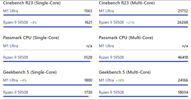
One oddity I find is that this mammoth chip isn't terribly faster then the 5950X, as such the 7950X will almost certainly be faster.
Source of the image and benchmarks.

1664717832309.png

With such a huge die size, increasing the GPU cores cannot continue, i.e., keep increasing the size of the die. Again, I don't see much advantages to Apple making a discrete gpu but I do think they're at a point of diminishing returns.
 

leman

macrumors Core
Oct 14, 2008
19,521
19,675
How much bigger can they really go with the the die size?

They still have quite some headroom. The M1 Max is around 400mm2, about the same size as the RTX 3070 die. Too-end Nvidia GPUs and Intel Xeons are much larger at over 600mm2.

With such a huge die size, increasing the GPU cores cannot continue, i.e., keep increasing the size of the die.

They will have to increase the clocks at some point if they want to keep going faster. The GPU is already large enough on itself, the Ultra has 8K compute units (will likely be 10k once the new generation hits). I fully agree that scaling the number of GPU cores much further will start getting awkward.
 
  • Like
Reactions: maflynn

deconstruct60

macrumors G5
Mar 10, 2009
12,493
4,053
Imagine how much bigger relative to M1 Ultra. Maybe 3D stack.


3D stack of an interposer? There is already present in the Ultra. 3D stack of very active silicon. Probably not.

A mainstream Desktop chip? How about a Epyc 7004 series (Genoa , Zen4 ) LGA 6096.

AMD-EPYC-Genoa-Zen-4-CPU-For-SP5-LGA-6096-Socket-Platform-1110x1480.jpg


AMD-EPYC-Genoa-Zen4-Backside-1536x1313.jpg


Or Intel Xeon SP gen 4 ( Sapphire Rapids ) LGA 4677


Intel-Architecture-Day-2021-Sailesh-with-Sapphire-Rapids-Close.jpg


Or with some 'local' HBM memory attached.

Intel-Vision-2022-Sapphire-Rapids-HBM-Top-2.jpg


[ Substantially less memory capacity via those HBM stacks. Tiered memory. ]


The Intel's solution is smaller because the packaging is more advanced ( 3D/2.5 interposers). Same would happen with Apple using and mild evolution of UltraFusion. AMD's packaging is cheaper.

But as pointed out, a large fraction of the Apple SoC package is going to be RAM. The semi-custom RAM packages for Pro/Max/Ultra already consist of 3D stacked RAM dies. That won't be new or likely to get much smaller.
 

deconstruct60

macrumors G5
Mar 10, 2009
12,493
4,053
How much bigger can they really go with the the die size?

One oddity I find is that this mammoth chip isn't terribly faster then the 5950X, as such the 7950X will almost certainly be faster.

The bulk of the Max/Ultra die space is allocated to GPU cores. So if test the Max/Ultra versus 5950X or 7950X on GPU computational tasks which one is faster?


With such a huge die size, increasing the GPU cores cannot continue, i.e., keep increasing the size of the die. Again, I don't see much advantages to Apple making a discrete gpu but I do think they're at a point of diminishing returns.

For what it is... Apple's die are not "Huge die size". You folks are compare packages which consists of different multiple dies sets aimed at different workloads. It is Apples to Oranges.

The overall Apple die packaging has limits. But what Apple has now isn't really at the borders of very 'big'.


Advanced%20Packaging%20Technology%20Leadership.mkv_snapshot_14.32_%5B2020.08.25_14.14.21%5D.jpg


Apple is using Info-LSI for M1 Ultra which is limited to approximately the 1x reticle limit. If they shifted over to CoWoS they could due 3x. ( 3 * ~ 800mm^2 --> ~ 2400 mm^2 ). Apple probably isn't going to put HBM memory stacks on this subassembly so they can use all of that for chiplets. Take that subassembly and use some less bleeding edge packaging for tight coupling to the LPDDR RAM modules. And done.

Doing twice a big as a duo (Ultra) is quite tractable ( 4 * ~430mm^2 -> ~1,800mm^2 ) . It is substantially more expensive, but well inside the boundaries of TSMC packaging. It won't fit in a laptop. And probably don't want to do "laptop" duo's for desktop only Ultras. I doubt Apple is going to try to compete on price with the mainstream generic GPU card market. So the additional expense probably will not be an issue for the customer target base they'll be going after. ( Apple isn't going to have some generic GPU market 'killer' product. They don't want one either. )

All they need is a 'desktop' oriented Max sized building block that is meant to scale up.

Also when N3 , N2 , 'N18A' , 'N16A' come along Apple will be able to squeeze incrementally more GPU cores into that same ~1,800mm^2 space.


The 'extreme' package with all the associated LPDDR modules won't be 'desktop' small. So not likely going to see a 'taller' Studio be the Mac Pro. They probably will need to go past the 7x7 inch footprint of the Mini (even if rotate the logic board vertical it still would present problems. And might as well let in some PCI-e slots as well since logic board passes the critical mass size. ) . The Xeon W-6200 inside the current Mac Pro is not some dainty sized package either. Chopping the current Mac Pro 'box' ( sans feet and handles) in half would still leave them plenty of room for a big, 5000mm^2 , package.

The affordability of the package ( 3D layout and chiplet development ) is a bigger constraint than the die size. If Apple gets the desktop chiplet set for the Studio , 'real' iMac Pro (not some iPad on a stick design), and Mac Pro then it is probably doable. Apple isn't going to create a 'killer' for multiple very high end dGPU performance zones. But single upper mid - entry high end range they can keep up with via a single multiple die package over time.

AMD's upcoming 7900 and 7800 are not monolithic dies either ( so not about die size). It is more about doing it more affordably. Apple trying to pound laptop optimized single, dies into scalable desktop class chiplets is a bigger problem than the size of the dies. That is the round peg into a square hole problem.
 
  • Like
Reactions: Boil

deconstruct60

macrumors G5
Mar 10, 2009
12,493
4,053
Do you think this would be a problem in practice or something that can be hidden by increasing the latency to hide the on-uniformity?

Can't really 'hide' latency from workloads that have real time processing timing constraints.
If this was trival then Metal would automagically hide the latencie between the GPU dies on a W6800X Duo coupled with Infinity Fabric. It does not. Nor does AMD present the two dies on a MI200 series GPU solution as one single GPU.


IMO the biggest practical issue will be RAM arrangement. If you connect these dies so that two sides touch, where does the RAM go?

On the outermost edges.


r2NZYcZWlaq7uVM4.jpg


There are two diagonal pairs here. ( MDF / EMIB multiple die fabric )

There is no UPI to allocate on an Apple die so throw that at memory controllers. Apple's is likely not so interested in quite so many PCI-e lanes also. So same thing. They just will not work so well as skinny rectangle laptop logic board SoC dies anymore.

Or use a scaled back UltraFusion to move the memory controllers off. ( both AMD 7900 series and Amazon Graviton 3 don't have memory controllers on same die as compute cores. Using 3D packaging can scale down the fan out size for the memory controllers connections to the outside world. (those don't scale as well as advance far process nodes becvause it is 'off' package . ) . Or a combination of those.


GPUs are just parallel processors. They don't have to communicate between each other much, just grab data from the memory and process it. It shouldn't really matter how close or far individual dies are for most things.

How 'far away' from the cores the memory is matters. Data in a L1 , L2 , or main RAM matters.
If have to take 'two hops' to get to remote memory controller than will cause synchronization issues when have very tight time constraints. That is why everyone has avoided multiple die GPUs until now. If it was "fall off a log" simple AMD , Nvidia , etc would have done it long ago and switched to smaller, cheaper dies.


P.S. Graviton 3


AWS-Graviton3-Processor-Cover.jpg


The chiplets on the bottom are for PCI-e and the four chiplets on either verticle side are for DDR5 . If toss the PCI-e chiplets could move the memory ones to left and bottom on picture and could do a 'four square' if wanted a mega package set up.

It is tough though to have "everything and the kitchen sink" as far as diverse I/O types and do a dense packed four square. but the memory aspect is tractable.
 
Last edited:
  • Like
Reactions: singhs.apps

diamond.g

macrumors G4
Mar 20, 2007
11,438
2,664
OBX
The bulk of the Max/Ultra die space is allocated to GPU cores. So if test the Max/Ultra versus 5950X or 7950X on GPU computational tasks which one is faster?
The Max/Ultra since the 5950X would be forced to use the CPU and the 7950X has a very small iGPU (2 CU RDNA2) so it would be faster than the 5950X (maybe) but far slower than Apple's SoCs.
 

leman

macrumors Core
Oct 14, 2008
19,521
19,675
Can't really 'hide' latency from workloads that have real time processing timing constraints.
If this was trival then Metal would automagically hide the latencie between the GPU dies on a W6800X Duo coupled with Infinity Fabric. It does not. Nor does AMD present the two dies on a MI200 series GPU solution as one single GPU.

These multi-GPU don’t have the bandwidth of Ultra Fusion nor are those dies designed to work as a single processor. If Apple connector works by joining together the internal fabrics of the dies, is it possible that it could really work like one big chip? I mean, huge chips do exist and have to manage communication between different units. But I also see how the complexity of a composite AS system must be staggering. Managing this many memory controllers and cache blocks must be a logistical nightmare.

Based on your expertise, how feasible is it to have multiple physically separate cache blocks to function as one big cache and what kind of requirements would a system of this kind impose? How are practical timing challenges solved in modern mesh interconnect systems where signal paths can have very different lengths and therefore propagation times?
 

senttoschool

macrumors 68030
Nov 2, 2017
2,626
5,482
One oddity I find is that this mammoth chip isn't terribly faster then the 5950X, as such the 7950X will almost certainly be faster.
Source of the image and benchmarks.
Please don't use Passmark and Cinebench as benchmarks for Apple Silicon. They're terribly unoptimized. In addition, Cinebench is just a bad CPU benchmark in general. Just search around the forum for why.
 

EntropyQ3

macrumors 6502a
Mar 20, 2009
718
824
These multi-GPU don’t have the bandwidth of Ultra Fusion nor are those dies designed to work as a single processor. If Apple connector works by joining together the internal fabrics of the dies, is it possible that it could really work like one big chip? I mean, huge chips do exist and have to manage communication between different units. But I also see how the complexity of a composite AS system must be staggering. Managing this many memory controllers and cache blocks must be a logistical nightmare.

Based on your expertise, how feasible is it to have multiple physically separate cache blocks to function as one big cache and what kind of requirements would a system of this kind impose? How are practical timing challenges solved in modern mesh interconnect systems where signal paths can have very different lengths and therefore propagation times?
Andrei Frumusanu made measurements of core-to-core latencies of Ryzen 3950/5950 before moving on. Interesting data.
It seems that, while acceptable for CPU loads, AMD deems it problematic at present for real-time graphics loads, as their new GPUs maintain a monolithic graphics die, only splintering off I/O.
 
Last edited:

senttoschool

macrumors 68030
Nov 2, 2017
2,626
5,482
Andrei Frumusanu made measurements of core-to-core latencies of Ryzen 3950/5950 before moving on. Interesting data.
It seems that, while acceptable for CPU loads, AMD deems it problematic at present for real-time graphics loads, as their new GPUs maintain a monolithic graphics die, only splintering off I/O.
Latency is more critical for CPUs than bandwidth. Opposite for GPUs. This is why multi-GPUs weren't made yet until the M1 Ultra. M1 Ultra is literally the first multi-die GPU.

AMD is rumored to be using a multi-die GPU as their next generation discrete GPU.
 

leman

macrumors Core
Oct 14, 2008
19,521
19,675
Andrei Frumusanu made measurements of core-to-core latencies of Ryzen 3950/5950 before moving on. Interesting data.
It seems that, while acceptable for CPU loads, AMD deems it problematic at present for real-time graphics loads, as their new GPUs maintain a monolithic graphics die, only splintering off I/O.

AMD uses a central IO die that routes all the communication between individual chips. That’s not the most latency-efficient multi-chip technology. Apples UltraFusion directly connects on-chip networks.

I disagree with your conclusion that AMD’s GPUs are monolithic because of the latency concerns. They are probably monolithic simply because that’s how AMDs technology works. In their current architecture the GPU is a single isolated device and they have no means (currently) to orchestrate workloads across multiple dies. This is easier with CPUs anyway as each CPU core is logically autonomous. Apple GPU tech does not have this limitation as shown by Ultra.
 
Register on MacRumors! This sidebar will go away, and you'll see fewer ads.