Become a MacRumors Supporter for $50/year with no ads, ability to filter front page stories, and private forums.

senttoschool

macrumors 68030
Nov 2, 2017
2,626
5,482
Those are the most favorable results for Intel that I’ve seen, but if I had to pick a workload that would shine in Alder Lake then one where you have a mix of heavier and lighter threads would be it (properly sent to the right cores of course). Gaming tends to fit that bill.
That's because the vast majority of people who buy DIY Ryzen/Core chips will use them primarily as gaming chips.

Mainstream laptop ADL will be tuned for efficiency more than raw performance.
 

cmaier

Suspended
Jul 25, 2007
25,405
33,474
California
That's because the vast majority of people who buy DIY Ryzen/Core chips will use them primarily as gaming chips.

Mainstream laptop ADL will be tuned for efficiency more than raw performance.
Fun fact: Most chips made by AMD and Intel are sold to consumers. At AMD we didn’t even think of consumers as ”our customers.” The vast majority of sales are to the OEMs. We did nothing to target our designs toward folks who were buying their own processors at Fry’s or what-not.
 

jinnyman

macrumors 6502a
Sep 2, 2011
762
671
Lincolnshire, IL
But the marketing of chips are towards DIY users. They are the trend setter or rumor creators who effectively do marketing for Intel and AMD. Why bother to come to CES and trying to be the best of chips in that era? Isn't that the whole point of marketing? Saying you wouldn't consider consumers as "customers", even though you worked for AMD is misleading. To make things for OEM to like, you have to make things for "consumers" to like.
 
  • Like
Reactions: senttoschool

mr_roboto

macrumors 6502a
Sep 30, 2020
856
1,867
But the marketing of chips are towards DIY users. They are the trend setter or rumor creators who effectively do marketing for Intel and AMD. Why bother to come to CES and trying to be the best of chips in that era? Isn't that the whole point of marketing? Saying you wouldn't consider consumers as "customers", even though you worked for AMD is misleading. To make things for OEM to like, you have to make things for "consumers" to like.
No, the portion of marketing visible to you is oriented towards DIY. @cmaier 's point is that DIY is not the primary trend setter for OEMs, and OEMs move far more units and are thus more important to AMD and Intel than any "influencer".

Yes, of course there is an indirect connection from end user to OEM to CPU designer. But the Dells and HPs of the world pay a lot less attention to the RGBZZZZZ crowd than you seem to think.

Here's an example of how it's really OEMs driving the bus: Iris Pro graphics. No gamer ever asked for that, they wouldn't be caught dead using an iGPU. It is generally thought to be a special feature Intel created at Apple's request, but also made available to other OEMs. It was expensive and never delivered performance as good as a dGPU. But Apple wanted to run their notebooks on a power efficient GPU most of the time, and they wanted that GPU to not completely suck.
 

mr_roboto

macrumors 6502a
Sep 30, 2020
856
1,867
They can use whatever benchmarks they want, all I am saying that the suite they use is useless for comparing the benchmark results. It's a bunch of random apps, some of which are specific to Linux, most have little relevance to real-world usage.
Yup. The main problem with Phoronix is that Michael Larabel's idea of how to run his website and test suite is "quantity >>> quality". He just wants to churn out tons of long articles and try to farm page views out of them. (Try visiting Phoronix without an adblocker sometime.) He's not putting much (if any) effort into test selection, careful interpretation of results, good controls to guarantee results are meaningful, etc. He just wants to hit "go" on whatever random comparison he's chosen to make (doesn't matter if the comparison even makes sense), wait for his scripts to churn out most of the article, toss in a few handwritten sentences, and push publish.

Similar problems abound in all his news stories. You are not going to get careful journalism or original insights from Phoronix, it's all very low effort.
 

senttoschool

macrumors 68030
Nov 2, 2017
2,626
5,482
Fun fact: Most chips made by AMD and Intel are sold to consumers. At AMD we didn’t even think of consumers as ”our customers.” The vast majority of sales are to the OEMs. We did nothing to target our designs toward folks who were buying their own processors at Fry’s or what-not.
Sure, you're making the best chips possible for your largest markets. That's the upcoming laptop ADL chips which are far higher volume. But I don't think a 12900k is targeted towards non-gamers. ?
 

Andropov

macrumors 6502a
May 3, 2012
746
990
Spain
The P cores of Alder Lake are essentially the P cores of Xeon SP Gen 4 ( Sapphire Ridge ). Those aren't "last minute" cores. The minor differences are the L3 cache size and I think the "advanced Matrix" unit ( which is a substantially separate 'part' of the core assembly. ). [***]

[***]. L2 vs L3

”…. There are some major differences between the consumer version of this core in Alder Lake and the server version in Sapphire Rapids. The most obvious one is that the consumer version does not have AVX-512, whereas SPR will have it enabled. SPR also has a 2 MB private L2 cache per core, whereas the consumer model has 1.25 MB. Beyond this, we’re talking about Advanced Matrix Extensions (AMX) and a new Accelerator Interface Architecture (AIA).
…..”

https://www.anandtech.com/show/1692...s-nextgen-xeon-scalable-gets-a-tiling-upgrade

‘major differences’ if looking for a server processor . But the 0.75MB is a significantly large die space difference . The baseline P core wasn’t designed to be laptop optimized.
The core design is not the part that feels rushed. I'm aware they reused core designs they were already working on (for both Golden Cove and Gracemont). But they ended up putting cores with mismatching ISA support (because that's what they had around), trying to fix it with a least common denominator approach disabling the AVX-512 instructions from the P cores (but not even fusing them off!) and then tried to hide the firmware option from motherboard manufacturers so they couldn't re-enable the AVX-512 instructions for the P cores. The two cores types were clearly not designed to work together in the same configuration. Also the whole scheduler situation.

Fantasy?

"... Individual chiplets are visible in this closeup of Meteor Lake test chips that pave the way to the PC processor's release in 2023. Intel's Foveros technology bonds the chiplets into 3D stacks. ... "


Intel is already prepping manufacturing of the packaging. It is past the fantasy stage. Gen 14 well past "tape in" and is in "tape out" state at this point. Isn't going to ship externally short term, but components are already being made in small numbers.
Tape out? The article says it's the *first* prototype! How could it be tapped out already? Also, the problem they had with 10nm was the yield, not that they were unable to make chips at all. Intel showed a working 10nm Cannonlake at CES 2017 (January), and we all know how long they needed to actually move their whole lineup to 10nm...
 
  • Like
Reactions: BigPotatoLobbyist

diamond.g

macrumors G4
Mar 20, 2007
11,437
2,665
OBX
Sure, you're making the best chips possible for your largest markets. That's the upcoming laptop ADL chips which are far higher volume. But I don't think a 12900k is targeted towards non-gamers. ?
Are any k series (unlocked cpu's) targeted at "normal users"?
 

deconstruct60

macrumors G5
Mar 10, 2009
12,493
4,053
I personally think AMD is done in the Windows laptop market. They'll be the budget option again. Intel is hyper aggressive right now; undercutting AMD on prices, spending billions to buy TSMC wafers at the same time as AMD or even before AMD, and releasing new architectures at an extremely rapid pace.

too early to write AMD off in laptop space. It isn't their priority, but they are not sitting still either.
iGPU wise they are still more than competitive with Intel iGPU. Apple's iGPU has "bent" the evaluation metrics for laptop iGPUs. AMD isn't on an even with Apple , but they are doing better than Intel.

The space were a system vendor can drop the laptop dGPU and just go with an iGPU is not the "budget laptop option" location.

AMD managed to get the TSMC N6 laptop discrete GPU out the door before Intel did. Intel is buying wafer but for the moment they are not shipping them. [ In part because working to get more solid drivers. ]

Intel is releasing new code names at a rapid pace. Not really new architectures. Rocket Lake got a new name more so to being backported from 10nm-class design to 14nm-class one. Alder Lake -> Raptor Lake probably is not a new architecture. "Raptor Cover" is pretty likely a cleaned up "Golden Cove" with the appropriate laptop and desktop revisions to from the server baseline design of Golden Cove. [ e.g. take out the stuff they are not using that bloats out the die space consumption. ] The 'little' , 'E' cores are reported to be exactly the same ( Gracemont) There is certainly no arch move there. Just lots more of them. ).

Here is a table from videocardz
"....
VideoCardz.comAlder LakeRaptor LakeMeteor LakeArrow LakeLunar LakeNova Lake
Launch DateQ4 2021Q4 2022Q2 2023Q4 2023Q4 20242025
Fabrication NodeIntel 7Intel 7Intel 4TBCTBCTBC
Big Core µArchGolden CoveRaptor CoveRedwood CoveLion CoveLion CovePanther Cove
Small Core µArchGracemontGracemontCrestmontSkymontSkymontDarkmont
..."

Golden Cove ~= Raptor Cove then have big/small covering two years. Lion Cove/Skymonth clearly cover two years. Intel has some more gap filling than AMD is doing , but the schedule above is basically a two year cycle on architectures.


Intel's bloated P cores and a relatively fixed laptop die space budget means Intel is taking a hit on space they can allocate to iGPU and other functions. if they shrink the P cores with "Raptor Cove" and then throw all of that, and more , at E cores, then they are not going to catch up in iGPU space.

AMD also put substantive effort into their latest generation into improving battery life in systems that use their chips.
AMD%20Product%20Premiere_Embargoed%20Until%20Jan%204%202022%20at%2011am%20ET%20%282%29-page-024_575px.jpg


AMD is on TSMC N6 and Intel is on N7. This is a step forward from the N7 they have been using. It isn't the N5 that will ship later this year , but it is shipping now. The laptop dGPUs from Intel and AMD probably lean in AMD's favor.


In short, Intel isn't offering the better CPU+GPU package system balance. Most of this "AMD is doomed" is coming myopic CPU drag racing benchmarks. Does AMD have a "Intel Killer" product offering and focus in the laptop space? No. Do they have enough to defend the position with will have carved out by the middle of 2022? Probably yes. Can Intel buy back a few percentage points? Probably. However, that won't be enough to squeeze AMD completely out as long as Intel trails in iGPU performance and AMD CPU cores are "good enough".


AMD probably knows better than Intel that going back to rely on the "budget" systems is probably a dead end.


Decent chance that Samsung implemented the RNDA2 architecture at least in part by themselves. There isn't a humongous leap between having just one X1 core and going to like 4 X1 and 4 710 cores and having a Windows 11 on Arm system to compete with Snapdraong 8cx gen 3 ( 4 X2 + 4 A78 )


Intel is willing to sacrifice its margins to put AMD back in the rearview mirror. I think they will succeed.

Intel is about to get into a battle with Nvidia on dGPUs. With TSMC in buying EUV ASML machines . With TSMC and Samsung on competing for contract fab design wins. With a AMD+Xlinix team up. Ampere/Amazon/etc on cloud services CPU packages. etc.

If all of that margin squeeze was only pointed at AMD that would be a bigger deal. However, like the old "Risk" game maxim goes ... don't get into a land war in Asia. Intel is fighting a broad front 'war' against multiple competitors at at he same time. A substantive chunk of Intel's margin scrafice is going to be stopping the "bleed" of percentage ; not buying it all back.


If AMD releases Zen4 in Q4 of 2022, it will mark 2 years since Zen3. In that same time, Intel will have gone from Tiger Lake to Alder Lake to Raptor Lake. Intel is targeting Meteor Lake in 2023.

As stated above. Raptor isn't a arch move. It is far more a "optimize" iteration than a "tick" (process ) or "tock" (architecture) one. Intel hand waving about how they are fully back on the tick-tock model probably wants to posture Raptor Lake as a "Architecture" move. It isn't.


Not sure why you think it's exotic. It's clear that the laptop/desktop world is heading towards big.Little. AMD is actually years behind Intel on this because Zen4 won't be big.Little. As a software developer, big.Little makes total sense to me even in high-power devices.

Has very little to do with the big.little classification and far more to do with the hefty multiple ratio between big.little cores. 8:8 -> 8:16 . The 16 is far more demonstrative that the big's are really suffering from being "too big". Going to something tagged as a 'little" or 'E' because they are being on fab node evolution to save die space at least as much to save energy.


Again, big.Little is here to stay. It's not exotic. big.Little has been mainstream on mobile for over a decade. It makes perfect sense for the vast majority of consumer workloads.

There is little justification why those ratios should be the same for desktop / laptop as they were for handheld mobiles that basically unused most of the time.


On a day to day basis, most consumers will notice a faster single-thread CPU more than a multi-CPU thread. big.Little allows Intel/Apple/ARM to design and implement a few really big high-performance cores and then let little cores work on background tasks.

What folks tend to notice more on their laptops is the battery life. Intel is throwing power consumption at hitting those single thread drag racing marks.

We'll see as the battery reviews come out for Gen 12 and Ryzen 6000 systems that are not high end gamer focused as to who is doing the better job at delivering better battery life.


In addition, Intel's E cores have the performance of Skylake at 1/3 the wattage. That's damn impressive as long as you don't compare to Apple Silicon.

Skylake was on 14nm 2014-6 and 2019-22 Gracemont cores are on Intel 7. If have a 50% node shrink , then about 50% of the power savings is pretty close to a "no brainer" competency demonstration and not "amazing". Intel put in some significant updated design work here. But they also are comparing back to a very old, relatively unoptimized node.
 
Last edited:

deconstruct60

macrumors G5
Mar 10, 2009
12,493
4,053

"... This theory is way out there, but it's plausible because AMD doesn't have a formidable low-power CPU core architecture to rival "Gracemont ..."

AMD wasn't 100% clear on how Bergamo was getting two 128 core counts. That could be very straightforwardly done with 16 core CCDs ( 8 * 16 = 128 ). So what AMD Zen 4c core would be is a core that allowed them to double up the number of cores on a single CCD of roughly about the same size or just incrementally bigger.

That seems more likely than Bergamo being some huge bloated CCD count solution ( e.g., 16 * 8 => 128 ).

There is a pretty good chance that the Zen4c isn't as comprehensive as the mainstream Zen 4 core. They are probably getting rid of something to crank the core count higher for a specifically selected set of workloads. (e.g., throw out high performance computing , matrix , and media while going after http server , double float javascript , and java. ). Also it won't be surprising if there are some clock caps on these also. Average data center workloads don't need max single thread drag racing speed . ( if have dozens of different active users juggling between then there are no "bursty" workloads where run and then the whole SoC goes to idle and then another race-to-sleep. )


There are a group of folks speculating that if AMD can make a mainstream Ryzen with a Zen2/3/4 CCD then they could make a consumer products with a Zen4c/5c/etc product. [ the Moorse Law Dead guy threw that spitball out there in a session with not much direct evidence driving it at all. ] I won't bet the farm on those theories. At least not without seeing how AMD 'cut down' the 4c.

Intel was suppose to do a "base station " sever of Gracemont with up to 24 cores to follow up the Atom P59xxB server products ( "Snow Ridge") . In 2020 that was suppose to be on the "old' Intel 7. Intel hasn't done high core count Atoms for consumers. That isn't really setting a trend for AMD to follow either.


Personally, I don't think that either Intel or AMD lives up to the hype. AMD CPUs have become more "fashionable" in the recent years, but the simply truth is that AMD has (mostly) caught up with Intel in terms of performance. As to Intel... I am not convinced with their approach. Golden Cove is IMO disappointing and as to the rest, Intel is simply throwing more cores at the problem. That is hardly sustainable.

If you are stuck on "N7" and your competitors are on "N5" it doesn't have to be sustainable; just a good enough stopgap. If with "Intel 4" they are still adding additional multiples to the E core count then yeah that is a problem.


The interesting stuff will start happening when the Meteor Lake and multi-chip module tech arrives. Until then they are just plugging the leaks on a rusty bucket.

Multiple chip arrives at the desktop/laptop level. Intel is already shipping evaluation/certification multi-chip to the big internet services providers.
 

BigPotatoLobbyist

macrumors 6502
Dec 25, 2020
301
155
They have 'data' in a sense, yeah, but it's mostly garbage data. You absolutely need to have the task priority annotated to be able to develop an accurate thread scheduler for a heterogeneous CPU architecture. There's no way around it, no matter how much ML or fancy keywords you throw at it. Garbage in -> garbage out.

One thing I agree with: Apple's vertical integration could be a bit overemphasized here (even by me when I have talked about it). While it's true that Apple has a great API to annotate thread priority, I'm not sure how widely used it is on macOS. On iOS it's commonplace, so scheduling is easier there, but on macOS there's many ways to develop a multithreaded app and GCD is just one of them. Sure, people who made a macOS app 'the Apple way' will have proper QoS on their threads, but multiplatform apps written for the UNIX world as a whole... probably not.

Ironically, Apple can afford to have a dumber thread scheduler. Since their E cores are comparatively slow, the scheduler only needs to prioritise between the P cores and the E cores when the CPU is at near-max throughput. There's no need to choose between the P and the E cores when the CPU is dealing with a medium-sized workload. The decision of which threads should be spilled to the E cores is comparable to the decision of which threads should be starved when a traditional, homogenous CPU reaches its maximum occupancy.

Intel needs to be smart when scheduling threads at medium-sized workloads, because their E cores are an integral part of their total performance. Some Alder Lake configurations will need to spill to the E cores at low (~40%) occupancy, so the decision of which thread goes in which core is critical. Incorrectly scheduling a high-priority task to a E core would result in such task being slower than in a 11th Gen CPU. If they can consistently schedule threads in the most optimal way, then great.


The A15 E cores are probably the most impressive. They're at A7X levels of performance while using A5X levels of power. They're insanely good.

SPECint-power.png


It'll be interesting to see how AMD approaches this. I have no doubt they'll have heterogenous cores at some point in the future, but I wonder if they're going to make them medium sized like Intel or if they are going to go for really small efficiency cores (or even for a 3-tier system, although I believe that's better suited for phones).
I do agree that Apple has more slack here. Mind you, that's also my point - a nontrivial portion of the success of the M1 et. Al has to do with the energy efficiency and absolute performance that can be realized by Apple's big cores. Hell, I think that Apple's A11 would prove superior or equivalent to Intel's Gracemont in many respects despite being fabricated on an aged TSMC 10NM process. It certainly has more IPC for most real-world integer workloads looking at the sub-benchmarks at respective clock rates.
 
  • Like
Reactions: Andropov

deconstruct60

macrumors G5
Mar 10, 2009
12,493
4,053
The core design is not the part that feels rushed. I'm aware they reused core designs they were already working on (for both Golden Cove and Gracemont). But they ended up putting cores with mismatching ISA support (because that's what they had around), trying to fix it with a least common denominator approach disabling the AVX-512 instructions from the P cores (but not even fusing them off!)

Why would a server core product that was "behind" its major competitors in core count have a fuse to turn off AVX-512. AVX-512 is one of the few features that allows Intel have lower core count but still remain competitive in HPC (high performance computing). Is there going to be any Xeon SP Gen 4 product with the AVX-512 switched off? Probably not. ( if AVX-512 doesn't work then flip off the whole core).

Second Tremont and Gracemont never had AVX-512 so it is puzzling why or how that mismatch would have "snuck up" on them. When work on Gracemont started it didn't have AVX-512. Intel went for a low common denominator AVX plus the AVX-VNNI ( AI/ML stuff).

The subunits are likely turned off.

This also fails to look at the whole Gen12 line up. In the middle of the i5 range you have this.


Which is a 6 P and zero E offering. Intel has a variety of customers and there many be a narrow few who don't want any "newfangled" E core that requires modifications to the OS scheduler ( i.e., not Windows but embedded OS systems ) . There can be custom motherboard that will only take a narrow subset of Gen 12 CPUs. Those board could get a different baseline firmware provided by Intel. ( If that is a very small set does it make sense to do two 100% segmented code build repositories for the firmware? NO. )


and then tried to hide the firmware option from motherboard manufacturers so they couldn't re-enable the AVX-512 instructions for the P cores. The two cores types were clearly not designed to work together in the same configuration. Also the whole scheduler situation.

If you leave the firmware settings the way Intel provided them in the reference designs and how they instruct you use them then there is zero problem. "Hide" is somewhat dubious connotation. If the code turns something off because you're not suppose to use it then if go in and hack the code to turn it back on then the hacker is causing the problem ; not Intel.


Tape out? The article says it's the *first* prototype!

Prototypical the package chip bonding technique and size specifics isn't "tape out" . Tape out is when send the design off to a fab unit to actually have wafers run and later chips from the wafer.

For the Foveros/EMIB process there is another chip that has to be created to serve as the interconnect channel between the dies. Then chips stacked on each other in very precise ways with smaller than 'normal' bonding. Both can be run concurrently. In fact if doing module chip package building then probably do want to run concurrent efforts.

Don't really need a 8B transistor chip to run tests to see if you aligned to dies together properly. Can check integrity and/or alignment of the chip to chip bonds with something much more simpler.

However, this also isn't a somewhat sloppy chip package that is much , much bigger than the die. Need to know final die sizes if going to dense pack them together with essentially not gaps. Probably would want to make some to confirm what the final sizes are going to be.


How could it be tapped out already?

Easily because there are two different things.

Also, the problem they had with 10nm was the yield, not that they were unable to make chips at all. Intel showed a working 10nm Cannonlake at CES 2017 (January),

Ice Lake's 10nm was not Cannonlakes "10nm". Yield is a symptom. It is not a cause or source of the problem. That "working" didn't include an iGPU.

if you go to ark.intel.com and search for "Cannon Lake" , Intel won't even show the page.

Intel mainly made these for a limited set of products

probably just to work out the metrics of the failure modes so they could guide the refinements. Pragmatically that was an "at risk" production that never went to high volume. Intel dailed back the density a bit , undid some of the exotic metal stuff they were doing , and a few other adjustments. One of the core problems was the recipe was too complicated.


and we all know how long they needed to actually move their whole lineup to 10nm...

That pretty much ignores the significant progress Intel made over last 2 years. The Ice Lake era 10nm ( basically 10nm+ ) isn't as good as SuperFin 10nm and certainly worse than Intel 7 ( Enhanced Super Fin 10nm ). The really should be a reset at 10nm and going forward. Yes Intel screwed up in that gap. No they are not following the same design decision paths as they were in that messed up period. It is like going back and now pointing at AMD saying they are doomed because Bulldozer had problem. That isn't the baseline they are using anymore.
 

deconstruct60

macrumors G5
Mar 10, 2009
12,493
4,053
. At AMD we didn’t even think of consumers as ”our customers.” The vast majority of sales are to the OEMs. We did nothing to target our designs toward folks who were buying their own processors at Fry’s or what-not.

This .... unlike Intel which has a dedicated overclocking lab....


https://www.anandtech.com/show/17220/interview-with-intels-dan-ragland-head-of-overclocking


the difference between the "folks buying their own processors" and "BubbaGump Neighborhood build shop" isn't all that great when the shop is relatively small. Technically the latter might be considered an OEM but they are more assemblers and making any component originally. the consumers and small shops aggregate up into groups that are overall bigger than more than a couple Mac desktop product categories.

AMD had no overall high share so 10-15% of a already small is ignorable. However, if hold 90% then 10-15% of that is substantively big enough market to pay attention to.

The "others" category has been steadily shrinking over time but still over 10%.


[ Some of the others is likely falling off into just build in-house. Similar to how substantive share of the server system sales are dropping out of buying from "big name" system vendors. ]
 

deconstruct60

macrumors G5
Mar 10, 2009
12,493
4,053
But the marketing of chips are towards DIY users. They are the trend setter or rumor creators who effectively do marketing for Intel and AMD. Why bother to come to CES and trying to be the best of chips in that era?

AMD and Intel go to CES and do not put their system vendors partner machines in their booth or their presentations? AMD and Intel at CES is a co-marketing event at least as much as it is a single vendor one. Systems sell with Intel or AMD stickers on them ( again co-sales-pitch .. drifting away from marketing analysis. )

A core component of CES is trying to get retailers stock what consumers might be interested in buying. Few average Joe consumers are actually walking out the convention hall with a new , significantly priced doo-dad in their goodie bag. Show big screen there so that Best Buy and Crutchfield stock it so some consumer buys it.


Isn't that the whole point of marketing? Saying you wouldn't consider consumers as "customers", even though you worked for AMD is misleading. To make things for OEM to like, you have to make things for "consumers" to like.

For large multiple thousand employee companies there is often a bit of a "blind men grabbing different parts of an elephant " effect. It is a 'tree' . it is a 'snake' ... The company is viewed through a peephole and don't really see the whole thing.

At the lower chip design layers , there can be a decent chance customer input has been encoded into more specific design constraints. These example code frags need to run faster. The die can only be so big (costs ). etc.
 

crazy dave

macrumors 65816
Sep 9, 2010
1,454
1,230
Why would a server core product that was "behind" its major competitors in core count have a fuse to turn off AVX-512. AVX-512 is one of the few features that allows Intel have lower core count but still remain competitive in HPC (high performance computing). Is there going to be any Xeon SP Gen 4 product with the AVX-512 switched off? Probably not. ( if AVX-512 doesn't work then flip off the whole core).

Second Tremont and Gracemont never had AVX-512 so it is puzzling why or how that mismatch would have "snuck up" on them. When work on Gracemont started it didn't have AVX-512. Intel went for a low common denominator AVX plus the AVX-VNNI ( AI/ML stuff).

The subunits are likely turned off.

This also fails to look at the whole Gen12 line up. In the middle of the i5 range you have this.


Which is a 6 P and zero E offering. Intel has a variety of customers and there many be a narrow few who don't want any "newfangled" E core that requires modifications to the OS scheduler ( i.e., not Windows but embedded OS systems ) . There can be custom motherboard that will only take a narrow subset of Gen 12 CPUs. Those board could get a different baseline firmware provided by Intel. ( If that is a very small set does it make sense to do two 100% segmented code build repositories for the firmware? NO. )


If you leave the firmware settings the way Intel provided them in the reference designs and how they instruct you use them then there is zero problem. "Hide" is somewhat dubious connotation. If the code turns something off because you're not suppose to use it then if go in and hack the code to turn it back on then the hacker is causing the problem ; not Intel.

I agree with @Andropov. The issue was that Intel put two cores with differing ISAs in a heterogeneous design which is a big no no right off the bat. Obviously the two cores were designed as they are, but just as obviously the idea to put them together came too late to properly redesign them and/or the solution around the AVX-512 vector units didn’t work. How do we know this?

1) initially Intel claimed AVX-512 would be enabled across their product stack moving forwards
2) then on Alder Lake Intel said AVX-512 would be enabled by turning the E-cores off and in any chip without E-cores
3) then Intel said AVX-512 would be fused off for every design including 0 E cores
4) then it turned out it wasn’t fused off and motherboard manufacturers were able to turn them on and while this was “unsupported” nobody at Intel stopped it and the motherboard manufacturers clearly manufactured boards with it supposedly on
5) then finally Intel issued new updates to turn the vector units off but for real this time


The entire thread is good but this is the best summary as it contains a screenshot of the Anandtech review. More below:


The above was written when Intel had told everyone that it was fused off (which was wrong). So the relevant section here is that just prior to Intel wrongly saying the vector units were fused off, Intel was putting out wrong information for development that AVX-512 was or could be fully enabled.

If Intel really had planned it to work out this way, they could’ve fused the offending vector units off but didn’t. If Intel had planned it this way their own developer documents wouldn’t detail how to get AVX-512 working on Alder Lake. If Intel had planned it this way they wouldn’t have allowed the OEMs to ship motherboards with it enabled by default and shipped to reviewers with it still functioning.

While the hybrid design went a good deal better in many ways than I think people were fearing (there was a lot of grim predictions about MS and Intel’s abilities to properly implement a thread director), Intel definitely screwed up on AVX-512. Another indicator that the hybrid was rushed is that CPUID leaves are screwed up between P and E cores such that migrating DRM or RV generation between core types could result in failure.

Thus, while Lakefield technically exists, in many ways Alder Lake is still a first generation heterogeneous CPU and it’s clear that not everything went according to plan in its design and development. Again, like @Andropov, to me, these are clear signs the hybrid part of the design was, at least in part, rushed. They had the cores they had and stuck them together to make them work. These are not cores that were designed from the beginning to work together. They did a pretty good job considering, but they made mistakes and those flaws will have to be improved upon in the next iteration.
 
Last edited:

BigPotatoLobbyist

macrumors 6502
Dec 25, 2020
301
155
The 125W setting means that they restricted the base power consumption (PL1), i.e. the CPU is only allowed to run at full turbo boost for short periods of time (PL2). In practice this often makes little difference in terms of performance, because most applications run in bursts rather than sustained maximum load; and when they are multi-threaded, the PL2 boost clock is more restricted anyway (because the maximum multi-core clock is lower than single-core). This is why it's misleading to only look at the peak boost power consumption of these CPUs.
Yes, and on the 12900K they really let loose on setting PL2=PL1 (roughly) by default in order to garner marginal benchmark gains at the cost of massive power consumption, so at least for desktops at high wattages it's not as bad as it would seem at first glance.

At lower power consumptions I am not convinced Alder Lake looks especially great relative to AMD solutions and certainly not ARM's (via MediaTek or Qualcomm) or Apple's.
 

BigPotatoLobbyist

macrumors 6502
Dec 25, 2020
301
155
Not sure why this is even a question. Of course they could. If you are willing to sacrifice power efficiency, there is significant clock frequency headroom. As TSMC demonstrated some years ago, you can clock an old Cortex A72 with 4.2GHz, which was maxing out in contemporary mobile designs at around 2GHz. And it is not just leakage but also dynamic power, as you would need to increase the voltage significantly.
My question isn't about the theoretical with regard to virtually any microarchitecture but namely the idea that wider architectures are difficult to clock high due to stalls and all, which seems to have been proven ********* due to Gracemont and Golden Cove alone (each having a 2x3 decode scheme and a 6-wide decode scheme, respectively) but it's not clear if there's something I'm missing.

Again, like you, my intuition is "no, there is not, the decode width and reorder depth does not impose a meaningful limitation if any".
 

BigPotatoLobbyist

macrumors 6502
Dec 25, 2020
301
155
They’re opposed because it’s Apple, simply put. Look through any comment section with a cross section of Apple news and gamers and you’ll see anti-Apple commentary everywhere. ARM is secondary to that.


Like any of those idiots overclock, lol. PCMR types are like car enthusiasts in that 98% of them are bench racing high performance stuff while daily driving econoboxes.


I’m just an armchair engineer, but that doesn’t necessarily mean they improved A15 as much as they could. i.e, they have the fastest mobile chip, and the second fastest is their gen before that, why would you increase speed again over battery life?

The case is different with the M series, with much larger batteries and tougher competition in performance.

And, from my viewpoint, most of the detractors from the M series has been critical of gpu performance. Where A15 saw a bigger leap iirc.

I think Apple has more room to grow than Intel here. I can’t imagine that they’re holding anything back.
Right, one thing to keep in mind is that even with TSMC's high-density cell libraries or whatever relatively lower power, high-density libraries Apple & Synopsys work on - the clock rates have been rising in the last few years due to TSMC progress it seems. See: the A15 on N5P node being pushed to 3.2GHz vs the A14 on 3GHz. Looking back: the A10, A11, A12, were all in the lower to mid 2GHz (e.g. 2.2-2.65GHz) range. Similar progression seen for Android phones. I think TSMC have some of their high-density stuff capable of hitting 3.4-3.7 the closer we get to N3 but I'd have to go back and look at their slides (in fairness these figures were for ARM reference IP but in principle the point stands).

With Apple's IPC, even taking the A15 microarchitecture as a constant and assuming no evolution (unlikely), increasing clocks 10% again would yield a more impressive performance improvement than it would for current Intel or AMD solutions, so they've got room to run on that alone.

But the counter to this is while marginal TSMC increases with the high-density designs are still occuring and Apple have room here (say the mid to upper 3GH range in the next few years) I doubt Apple will be interested in fabricating M-series chips on say an HPC library like N4X with massively increased leakage just to compete with Intel and AMD in the 4-5+ GHz ranges anytime soon, whereas those two among others will certainly evolve their microarchitecture(s) still and increase SRAM sums etc.
 

BigPotatoLobbyist

macrumors 6502
Dec 25, 2020
301
155
Zen 3 is a year old and Zen 4, barring delays, will be here at the end of the year. That’s a reasonable cadence. Intel’s next chip Raptor Lake will be a reorganized Alder Lake similar to A15 relative to A14. It’s important to remember how much ground AMD had to catch up to Intel, that Zen 3 surpassed them by as much as it did surprised everyone, including AMD. Further AMD does have Zen 3+ coming to the desktop soon. For laptops they’re still competitive in terms of perf/W. Finally it’s important to remember that Intel’s total solution is not quite as cheap as it first appears: DDR5 is expensive and necessary if Alder Lake’s cores are to actually stretch their legs and motherboard prices have gone up.

The issue is that Alder Lake’s Golden Cove cores are still too big and power hungry to match AMD in core count. AMD’s performance cores are still too far ahead of Intel’s here. Thus Intel introduced midrange Gracemont cores to up the number of cores that could fit on a single die without blowing up power or die size. Now these midrange cores are actually quite nifty but should not be confused with traditional little or E-cores. This is what @Andropov and @leman were trying to explain earlier in thread with @senttoschool. Yes Alder Lake is heterogeneous in core size (and unfortunately ISA, that’s one indicator that Alder Lake’s design was a bit rushed), but Intel’s heterogeneity’s raison d’être is different from say Apple’s. In some ways it is more similar to ARM’s tri-level designs … just without the little cores. The focus of such midrange cores is on multithreaded throughput perf/W while the focus of little cores is to as efficiently as possible keep housekeeping threads off the main cores. Midrange Gracemont and A7x cores *can* do that housekeeping just as A5x and Icestorm cores can be used for multithreaded throughput. But in neither case is it their primary function. (Icestorm is a weird case because it actually exists somewhere between A5x cores and A7x cores. But that’s a whole ‘nother topic.) Bottom line is though: while AMD may adopt heterogeneous CPUs they don’t face quite the same problems as Intel. They might decide that it also makes sense to go with midrange cores for themselves but they might not.

Overall I wouldn’t put the relationship between Intel 12 Gen and AMD Zen 3 as a lack of progress from AMD but Intel finally unf***ing themselves and moving to counter AMD’s surprise resurrection.
This is precisely the case. Intel wanted an area-efficient (preserve margins) way to compete with AMD in peak throughput, and since there are diminishing (though worthwhile in a sense) returns to additional logic structures for a single core, slicing off the disproportionate expense for a smaller core microarchitecture & fabbing multiple of them on low voltage (denser) libraries offers greater throughput, and the ratios are reportedly 4 small cores for every big core.

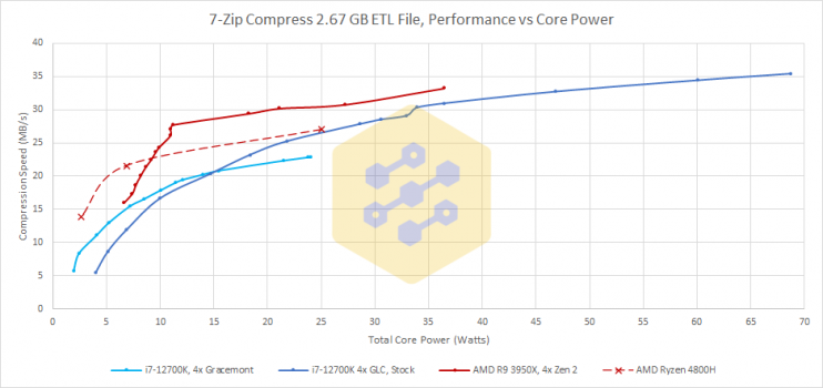
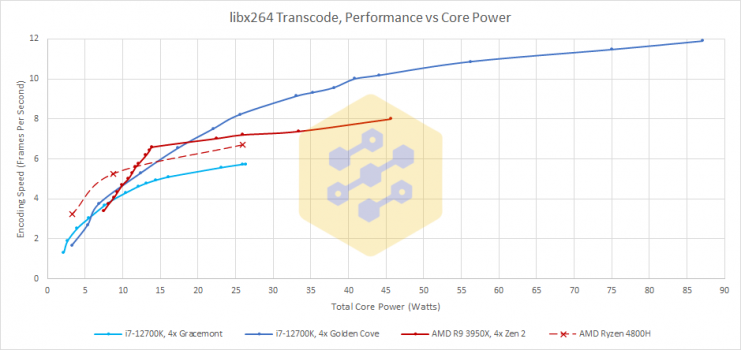
The other upswing is the idling efficiency or energy efficiency in modest frequency ranges. Gracemont in 2-3GHz on integer workloads is an improvement upon Golden Cove's energy efficiency — particularly at limited wattages depicted in the graphs below from Chips & Cheese. Still, the margin of gain here is not remotely as sizable as is often believed, because morons really thought Intel would have an ARM A7X-tier core, which was obviously ********, and in many cases the Golden Cove cores are just flat out more energy efficient.

Which brings us to another point, one way in which ADL's Gracemont can actually harm efficiency in default configurations is in to pushing the Gracemomt cores too hard, since their optimal V/F curve & IPC is not friendly to 3-4GHz. Therefore, the 3-3.8GHz range is not at all energy efficient for Gracemont relative to Golden Cove.

Hell, even Zen 2 Renoir beats it in two separate contexts all across the curves and at much lower clock rates. Naturally, I am not surprised by the Gracemont vs Golden Cove results, as I've maintained they were primarily an area play from the start (even referring to Intel's own graphs) — but it's pretty pathetic that four Gracemonts show out this goddamn poorly vs... Zen 2 Renoir?


Attachments

  • D2CD7734-5697-40C1-9387-8AFCB3E47B48.png
    D2CD7734-5697-40C1-9387-8AFCB3E47B48.png
    16.2 KB · Views: 46
  • D77F1747-52BA-4F0E-8245-C46A07B4674A.png
    D77F1747-52BA-4F0E-8245-C46A07B4674A.png
    15.6 KB · Views: 50
Last edited:

BigPotatoLobbyist

macrumors 6502
Dec 25, 2020
301
155
Not sure why this is even a question. Of course they could. If you are willing to sacrifice power efficiency, there is significant clock frequency headroom. As TSMC demonstrated some years ago, you can clock an old Cortex A72 with 4.2GHz, which was maxing out in contemporary mobile designs at around 2GHz. And it is not just leakage but also dynamic power, as you would need to increase the voltage significantly.
Right though mind you the dynamic power is a given. The leakage is the component that (especially given the design itself would change e.g. they'd need to utilize different libraries on current process nodes) is non-obvious to many.
 

MayaUser

macrumors 68040
Nov 22, 2021
3,178
7,204

Rigby

macrumors 603
Aug 5, 2008
6,257
10,215
San Jose, CA
Yes, and on the 12900K they really let loose on setting PL2=PL1 (roughly) by default in order to garner marginal benchmark gains at the cost of massive power consumption, so at least for desktops at high wattages it's not as bad as it would seem at first glance.

At lower power consumptions I am not convinced Alder Lake looks especially great relative to AMD solutions and certainly not ARM's (via MediaTek or Qualcomm) or Apple's.
I think Intel will easily beat Mediatek and Qualcomm CPUs in terms of power efficiency, if that comparison even makes sense (remember, power efficiency is not the same as low absolute power consumption). Where it lands relative to the M1 remains to be seen when we have better data. I think the most efficient Alder Lakes will be the P and U versions, which according to Intel engineers are optimized for power, while the H parts seem to have the same performance-oriented profile as the desktop parts.
 
Register on MacRumors! This sidebar will go away, and you'll see fewer ads.