Become a MacRumors Supporter for $50/year with no ads, ability to filter front page stories, and private forums.

name99

macrumors 68020
Jun 21, 2004
2,410
2,322
I know TFLOPs don't translate in fps, but the Z1 has like 3 times the TFLOPs of the M2. Something went wrong with the benchmark.
Maybe, maybe not.
TFLOPs is basically the GHz of the GPU world. TFLOPs is not *completely* meaningless, and can tell you a lot within a single product family, or even from one generation to the next; but it's an extremely limited metric.
In the GPU case, among other things it misses:
- memory issues (bandwidth and latency)
- GPU "parallelism" issues – how expensive is it to start a new kernel? to what extent can multiple kernels execute simultaneously? how expensive is synchronization? how good is the scheduler? etc etc
- and this is even BEFORE we get into graphics-specific stuff, and issues like different graphics "models" (both the APIs and their relative expressivity/cost; and things like tiled vs non-tiled)

I'm not saying something didn't go wrong with the test; I'm simply saying that asserting "TFLOPs therefore better" is a lousy argument.
 

name99

macrumors 68020
Jun 21, 2004
2,410
2,322
RDNA3 TFLOP is assuming you are able to dual issue FP32 across the SIMD's. Most games/benchmarks don't, so you are leaving like "half the performance" on the table (so to speak).
Is this because it's inherently difficult to create SIMD2 ops? That seems like a compiler flaw that should easily be fixable in the context of graphics, by conceptually imaging a warp as 128 wide and mostly compiling it that way?

Or is this a consequence of (ah the joy of the PC world) people using code that hasn't been recompiled in five years, so it doesn't even know about the existence of the FP32 SIMD2 operations?
 

name99

macrumors 68020
Jun 21, 2004
2,410
2,322
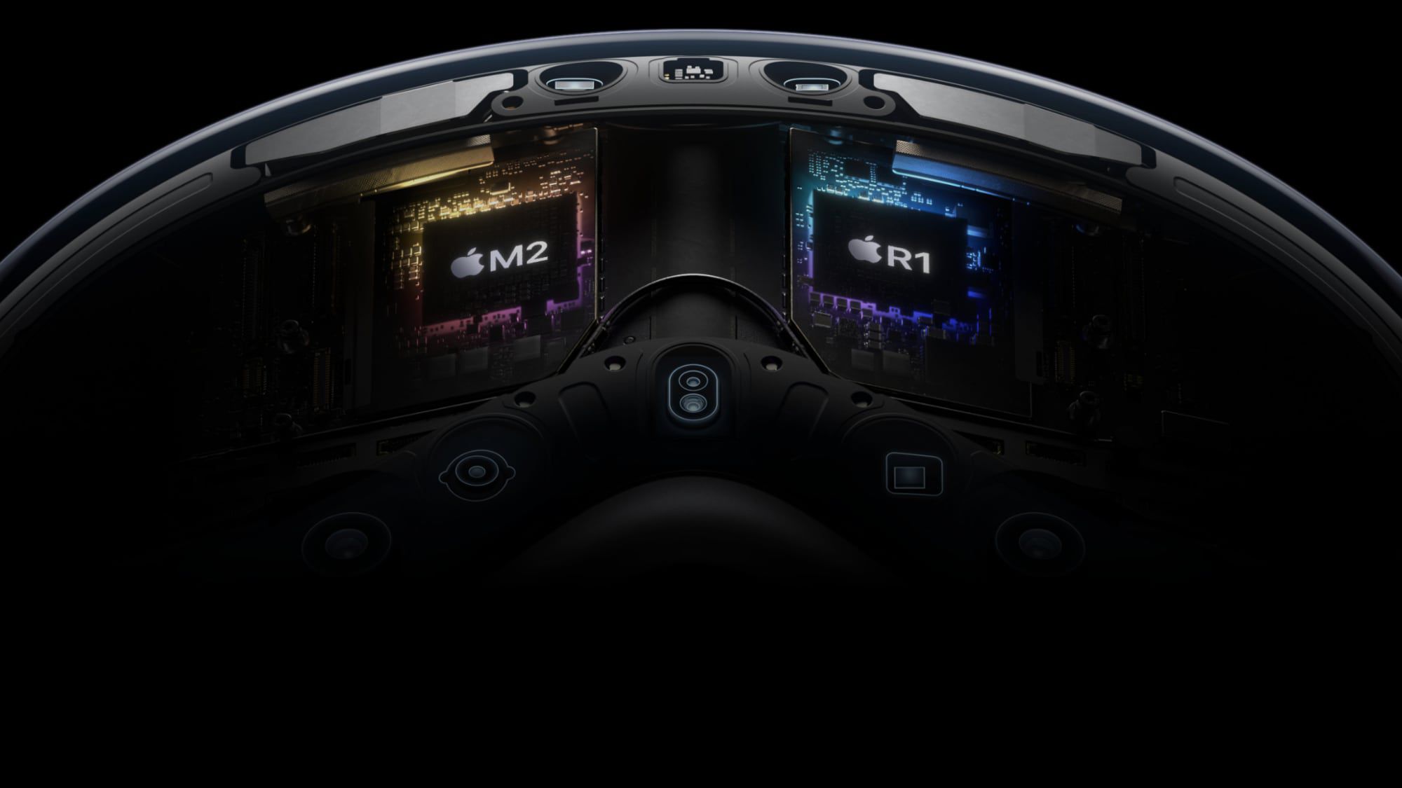
In the talk Srouji talks about how the Watch SoC was done at one of the Isreali R&D centers. The Vision Pro has the R1 chip. You don't need much speculation to see there are 'cousins' of the M-series sequence. Or that there are more than just the plain M1 ( Pro , Max , Ultra ) . He also said get into the hands of 'millions and millions'. An "extreme" is not going to get into the hands of 'millions and millions' at all.

Apple has 'A' , 'M' , 'R' , and 'S' series of SoCs. That is an extended family. No need to make up something else. And pretty good chance Apple expand much from that breadth at all. [ Again the video of hiring selectively and for stuff to make unique stuff for Apple products. Coupled with Apple's re-use deployment in systems. 'M' in both Macs and iPads. 'A' in both phones , iPads , and AppleTV. 'S' in watch and Homepods . etc. etc. The 'R' is probably only temporarily an outlier ( if boondoggle Apple Car showed up ... good chance it would get tossed into it. ). ]
You're assuming that R is the same sort of thing as A, M and S. I don't know that that's true. A better analogy might be something like the U or H, in that it's doing a very different sort of job and, while packed full of logic, that logic does not correspond to what we'd think of as a CPU or a GPU.

We really have no idea what the R1 actually does. It seems like a combination of fancy ISP (modify the incoming images) and Display Controller (tweak the outgoing images). Reuse in an Apple car seems plausible, but who knows?
Is it mostly "just" bigger versions of existing Apple IP? Or are there important and difficult algorithms embedded in there that we don't know about?

Crazy idea (for example) – would it make sense for Apple to sell an Apple Camera as a high-end DSLR, reusing, eg the R1 as part of the magic to make this a camera prosumers would lust after (and pay more for than a usual DSLR)???
Maybe DSLR-like in terms of stills – but also Red-like in terms of video...
 

NT1440

macrumors Pentium
May 18, 2008
15,092
22,158
You're assuming that R is the same sort of thing as A, M and S. I don't know that that's true. A better analogy might be something like the U or H, in that it's doing a very different sort of job and, while packed full of logic, that logic does not correspond to what we'd think of as a CPU or a GPU.

We really have no idea what the R1 actually does. It seems like a combination of fancy ISP (modify the incoming images) and Display Controller (tweak the outgoing images). Reuse in an Apple car seems plausible, but who knows?
Is it mostly "just" bigger versions of existing Apple IP? Or are there important and difficult algorithms embedded in there that we don't know about?

Crazy idea (for example) – would it make sense for Apple to sell an Apple Camera as a high-end DSLR, reusing, eg the R1 as part of the magic to make this a camera prosumers would lust after (and pay more for than a usual DSLR)???
Maybe DSLR-like in terms of stills – but also Red-like in terms of video...
I think it’s safe to say the R1 is all about “sensor fusion” using a realtime-OS.

It’s purpose is to take the huge amount of input coming from all the cameras and other sensors, make decisions on what’s needed and deliver it to the GPU of the M2 for drawing onto the screens.

There have been quite a few mentions of “sensor fusion” as a major focus from Apple over the recent years, including job postings specifically for it.

The R series is definitely going to be a thing to keep an eye on for use in other products going forward.
 

Chuckeee

macrumors 68040
Aug 18, 2023
3,065
8,730
Southern California
I'm not saying something didn't go wrong with the test; I'm simply saying that asserting "TFLOPs therefore better" is a lousy argument.
I agree. In addition, I thought the definition of what actually constitutes an “operation” with respect to defining FLOP was still fuzzy. What combinations of shifts, additions and multiples at what level of precision is not firmly established. Lots of room to “game” the benchmark to make a specific manufacturer look better

For a while (I seemed to remember from the 1980-1990’s) there was an effort to standardize on a 32-bit butterfly transform but it was strongly opposed by processor developers since their processors weren’t optimized for that but they wouldn’t discloses what operations they use for their FLOP benchmarks since that was “proprietary”. You could always buy their processor and do your own test.
 

theorist9

macrumors 68040
May 28, 2015
3,880
3,060
You know, just being optimistic. Single-monitor support has been a recurrent point of criticism for the base M1/2, and given that Apple now managed to fit external display support onto A17 it could be possible that they will improve it on M3. Then again, there doesn't have to be any correlation.
TIL I learned this interesting factoid, from Simon Jary of Macword:

"Indeed, in its M1 and M2 MacBooks tech specs, Apple doesn’t even call it Thunderbolt 4, listing it as “Thunderbolt / USB 4” including Thunderbolt 3. For the superior M1 Pro and M1 Max MacBook Pro models, Apple lists the ports as full Thunderbolt 4—this is likely because the Pro/Max versions of the M1 can support multiple external screens, unlike the limited plain M1 or M2 MacBooks. Without the ability to connect to two external displays, it can’t be labelled as Thunderbolt 4.....Thunderbolt 3 was required to support only one external 4K monitor, whereas every Thunderbolt 4 laptop has to support two 4K displays or one 8K display." [emphasis mine]


  • Like
Reactions: Xiao_Xi

Jamie I

macrumors newbie
Jan 16, 2023
19
67

Attachments

  • IMG_2428.jpeg
    IMG_2428.jpeg
    123.8 KB · Views: 105
  • Like
Reactions: APCX and Mac_fan75

Jamie I

macrumors newbie
Jan 16, 2023
19
67
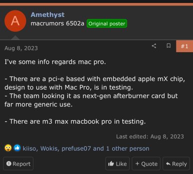
There is some news from Amethyst (leaked Mac Studio)

There is supposed to be PCIE modules embedded with M series chip designs and it’s being tested in the M2 Ultra Mac Pro right now.

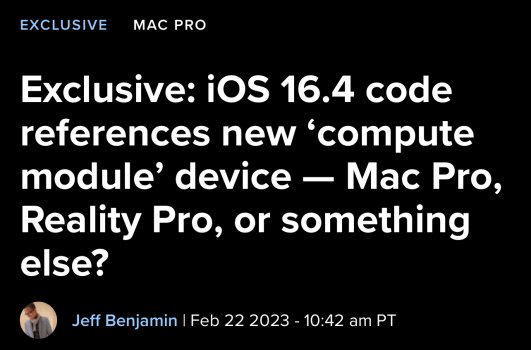
That’s probably why ComputeModule 13,1 and ComputeModule 13,3 were found in iOS 16.4 beta earlier this year
 

Attachments

  • IMG_2273.jpeg
    IMG_2273.jpeg
    260.7 KB · Views: 120
  • IMG_2431.jpeg
    IMG_2431.jpeg
    360.9 KB · Views: 117
  • Like
Reactions: scottrichardson

diamond.g

macrumors G4
Mar 20, 2007
11,438
2,665
OBX
Is this because it's inherently difficult to create SIMD2 ops? That seems like a compiler flaw that should easily be fixable in the context of graphics, by conceptually imaging a warp as 128 wide and mostly compiling it that way?

Or is this a consequence of (ah the joy of the PC world) people using code that hasn't been recompiled in five years, so it doesn't even know about the existence of the FP32 SIMD2 operations?
AMD more or less did the same thing nVidia did with Ampere and made their Vector Units capable of doing FP32+FP32 or FP32+INT32. nVidia's is a little bit different because the made half their SMs around the FP/INT ability. AMD seems to have made it so all their VU's can do this.

So far it seems like a compiler/scheduler (driver?) issue that utilization of this "dual issue" of FP32 isn't really used. And it also "neatly" explains why the gains from RDNA2 aren't as big as they were purported to be. CASE: it is why the 7900GRE isn't much faster than the 6950XT even though the 7900GRE has twice as many TFLOPs.

1696933436617.jpeg
 

leman

macrumors Core
Oct 14, 2008
19,521
19,677
Maybe, maybe not.
TFLOPs is basically the GHz of the GPU world. TFLOPs is not *completely* meaningless, and can tell you a lot within a single product family, or even from one generation to the next; but it's an extremely limited metric.

I think that TFLOPs for GPUs is probably more useful than Ghz for CPUs, simply because GPUs are fairly simple in-order machines with comparable IPC (at least on FP32 data) and very similar operation. Effective bandwidth for GPUs from the same category tends to be comparable and while I agree with you that kernel launch latency/sync latency can be very important for some tasks, it tends to be less of an issue for graphics.

Is this because it's inherently difficult to create SIMD2 ops? That seems like a compiler flaw that should easily be fixable in the context of graphics, by conceptually imaging a warp as 128 wide and mostly compiling it that way?

Well, AMD's SIMD2 instruction (VOPD) is subject to some strict rules which registers can be used etc., so I can imagine that using it in practice might prove challenging.

You can find more info here: https://www.amd.com/content/dam/amd...r-instruction-set-architecture-feb-2023_0.pdf

Or is this a consequence of (ah the joy of the PC world) people using code that hasn't been recompiled in five years, so it doesn't even know about the existence of the FP32 SIMD2 operations?

The shaders are compiled by the driver on the host machine, so that's unlikely.

AMD more or less did the same thing nVidia did with Ampere and made their Vector Units capable of doing FP32+FP32 or FP32+INT32. nVidia's is a little bit different because the made half their SMs around the FP/INT ability. AMD seems to have made it so all their VU's can do this.

That's not how I understand it. And I also find the marketing slide you posted a bit confusing since it appears to contradict what AMD is saying in their manual (e.g. the slide suggested that they can dispatch a full wave64 per cycle, while the manual says that wave64 is dispatched over two cycles).

Anyway, the way I understand it (doesn't have to be right of course) is that AMD added a second 32-wide SIMD to each previous SIMD, but didn't really change the plumbing much (register file etc.). So they can execute a second operation, but they can't fetch all the data from the register file. Don't ask me for the details how this works exactly, I don't understand it.

Also, I've read somewhere that Nvidia has a similar limitation (no idea if it's as severe), as a pair of their SIMD shares the same register file, but Nvidia is able to work around it a bit better since they schedule the operation from different kernels. Sometimes this results in an additional stall, but Nvidia has enough compute to compensate for this. In general, Nvidia's units are simpler, while AMD does this additional packed SIMD within SIMD thing.
 
Last edited:

APCX

Suspended
Sep 19, 2023
262
337

Poor testings as it seems he did not connect the power cable to the Razer laptop which is too obvious just like others mentioned.
You should probably retract this given the creator of that testing video has confirmed the Razer laptop WAS plugged in.
 

name99

macrumors 68020
Jun 21, 2004
2,410
2,322
AMD more or less did the same thing nVidia did with Ampere and made their Vector Units capable of doing FP32+FP32 or FP32+INT32. nVidia's is a little bit different because the made half their SMs around the FP/INT ability. AMD seems to have made it so all their VU's can do this.

So far it seems like a compiler/scheduler (driver?) issue that utilization of this "dual issue" of FP32 isn't really used. And it also "neatly" explains why the gains from RDNA2 aren't as big as they were purported to be. CASE: it is why the 7900GRE isn't much faster than the 6950XT even though the 7900GRE has twice as many TFLOPs.

View attachment 2292312
You're not answering the real question - to what extent is the code used on these new AMD architectures recompiled to take optimal advantage of these new operations? (And of course the same for nVidia and Intel.)
I could very much believe, because this is how the PC world does things, that code from five years ago is finalized by the driver, so, yeah it "works", but it has in no sense been compiled to be optimal for the design.
 
Last edited:

name99

macrumors 68020
Jun 21, 2004
2,410
2,322
Well, AMD's SIMD2 instruction (VOPD) is subject to some strict rules which registers can be used etc., so I can imagine that using it in practice might prove challenging.

You can find more info here: https://www.amd.com/content/dam/amd...r-instruction-set-architecture-feb-2023_0.pdf

The shaders are compiled by the driver on the host machine, so that's unlikely.
Everyone seems to be missing the point here.
The source code is compiled to some sort of intermediate representation on the DEVELOPER's machine. That intermediate representation is finalized by the driver to the precise details of the target GPU. But the finalizer is not an optimizing compiler; it's more like an assembler.
If the intermediate code was not optimized for a particular type of target (eg the compiler had no reason to even attempt to place together operations that could operate as SIMD2) then the finalizer can't do much to fix this.
It's like op fusion – the CPU does what it can with the instruction stream, but to work well the compiler needs to KNOW what operations will be fused so that those operations are placed sequentially in the stream.

My *guess* is that this exploiting these operations is not that hard for the compiler – but it does require the compiler used to actually be the most recent version of the compiler! That's the issue I keep trying to get at the root of – are these benchmarks even compiled with a modern enough compiler?

The same is of course true for the CPU, just not nearly as much so. I expect all the CPU benchmarks to improve slightly (via higher IPC) when GB et al are recompiled with a compiler that incorporates knowledge of things like new op fusions (or the new branch optimizations) in the A17.
 

leman

macrumors Core
Oct 14, 2008
19,521
19,677
Everyone seems to be missing the point here.
The source code is compiled to some sort of intermediate representation on the DEVELOPER's machine. That intermediate representation is finalized by the driver to the precise details of the target GPU. But the finalizer is not an optimizing compiler; it's more like an assembler.
If the intermediate code was not optimized for a particular type of target (eg the compiler had no reason to even attempt to place together operations that could operate as SIMD2) then the finalizer can't do much to fix this.
It's like op fusion – the CPU does what it can with the instruction stream, but to work well the compiler needs to KNOW what operations will be fused so that those operations are placed sequentially in the stream.

Is this really the case though? The intermediate formats I am aware of use fairly high-level SSA representation. The initial compiler only performs basic optimisations (eliminating dead code, common subexpression elimination etc.). The final optimisation passes (e.g. dependency analysis and register allocation) will be done by the driver.

Besides, I am not aware of any shader compilers trying to optimise for certain GPU architectures. Well, Apple does, but the IR they generate is much closer to the machine. On the other hand SPIR-V is still essentially a high-level language, and specific u-arch optimisations are the drivers job.
 
  • Like
Reactions: Basic75

name99

macrumors 68020
Jun 21, 2004
2,410
2,322
That's not how I understand it. And I also find the marketing slide you posted a bit confusing since it appears to contradict what AMD is saying in their manual (e.g. the slide suggested that they can dispatch a full wave64 per cycle, while the manual says that wave64 is dispatched over two cycles).

Anyway, the way I understand it (doesn't have to be right of course) is that AMD added a second 32-wide SIMD to each previous SIMD, but didn't really change the plumbing much (register file etc.). So they can execute a second operation, but they can't fetch all the data from the register file. Don't ask me for the details how this works exactly, I don't understand it.

Also, I've read somewhere that Nvidia has a similar limitation (no idea if it's as severe), as a pair of their SIMD shares the same register file, but Nvidia is able to work around it a bit better since they schedule the operation from different kernels. Sometimes this results in an additional stall, but Nvidia has enough compute to compensate for this. In general, Nvidia's units are simpler, while AMD does this additional packed SIMD within SIMD thing.
This is unclear to me.

The basic AMD pathway going forward, as far as I can tell, is that on the Mi side they seem to believe (probably correctly) that they can't win against nVidia in the AI space, so there's no point in following nVidia into the realm of FP8 and designs optimized for these tiny data elements;
instead what they CAN do is be better than nVidia for the space of HPC, engineering, and basically all STEM work that isn't AI. Thus design Mi with the baseline compute element as FP64 rather than FP32, and make minor modifications so that it can also operate on an FP32 SIMD2 element.

That's Mi. The question then is to what extent do they reuse this particular design element across the entire line. All of CDNA? Kinda makes sense. Also for RDNA? Hmm, well that's the question.
AMD have redesigned this stuff so often (like 5 times in the last 15 years; very unlike nV) that simply going on how they did it two years ago doesn't really answer the question of how they are doing it right now or will do it in the next design.

As for nV, their path has been slightly different. I forget the details but
- I don't think they have any FP32 SIMD2 handling to better exploit their FP64 units.
- what they do have is FP16 SIMD2 handling.
- BUT recent nV handle FP16 operations in the tensor cores, not in the "mainline" FP32 cores.

And of course the point I keep making about compilers. nV's compilers have been at this for longer, so if I take random code compiled 4 yrs ago, the nV code may well have been compiled to optimize for SIMD2, whereas the AMD code may not have been.

And for both cases, yeah, I'm constantly shocked at how non-generic their high level scheduling is. The designs still seem to be "modal" in various ways, with terrible ability to schedule multiple simultaneous different kernels – kinda like if a CPU had an FP mode and an integer mode, and you couldn't cheaply context switch between an integer app and an FP app. Certainly on the nV side they have been boasting about fixing this in every new design for about ten years – and every time I look at the fine print, there's always yet more BS that constrains the actual extent of the simultaneity allowed! As far as I can tell, Apple is much more forgiving in this respect, much less modal; but that's an impression from reading the patent stream (and the way they seem to punch above their weight in certain benchmarks), I'm not absolutely certain of this.
 

name99

macrumors 68020
Jun 21, 2004
2,410
2,322
Is this really the case though? The intermediate formats I am aware of use fairly high-level SSA representation. The initial compiler only performs basic optimisations (eliminating dead code, common subexpression elimination etc.). The final optimisation passes (e.g. dependency analysis and register allocation) will be done by the driver.

Besides, I am not aware of any shader compilers trying to optimise for certain GPU architectures. Well, Apple does, but the IR they generate is much closer to the machine. On the other hand SPIR-V is still essentially a high-level language, and specific u-arch optimisations are the drivers job.
I would not call either dependency analysis or register allocation optimization. I'm thinking of large-scale structural optimizations like the granularity of a loop.
eg Why unroll a loop to handle two elements per iteration if there's no need to do so? But it's that two-wide unrolling that makes a SIMD2 use case visible...
 

leman

macrumors Core
Oct 14, 2008
19,521
19,677
The basic AMD pathway going forward, as far as I can tell, is that on the Mi side they seem to believe (probably correctly) that they can't win against nVidia in the AI space, so there's no point in following nVidia into the realm of FP8 and designs optimized for these tiny data elements;
instead what they CAN do is be better than nVidia for the space of HPC, engineering, and basically all STEM work that isn't AI. Thus design Mi with the baseline compute element as FP64 rather than FP32, and make minor modifications so that it can also operate on an FP32 SIMD2 element.

I didn't look at the Mi, so can't comment on that, I'll just trust your judgement.

But AMD certainly is going to try to compete with Nvidia in the AI space. Until now their recipe has been making their SIMDs more flexible (they can either work as 32 32-bit SIMDs, or 64 16-bit SIMDs. Since the programming model is still SIMT (or one thread per SIMD lane), you are essentially getting packed SIMD capabilities within each lane. Again, that's what you write as well, I just want to make sure we are on the same page here.

Anyway, I won't be surprised if they also add packed FP8 or something like that in new generations. They already have instructions that operate on the entire SIMD (stepping out of the SIMT model for a moment) to do matrix multiplication. This could be enhanced with additional data formats or even sparsity.

As for nV, their path has been slightly different. I forget the details but
- I don't think they have any FP32 SIMD2 handling to better exploit their FP64 units.
- what they do have is FP16 SIMD2 handling.
- BUT recent nV handle FP16 operations in the tensor cores, not in the "mainline" FP32 cores.

Nvidia used to have packed FP16 SIMD2, but they dropped it when they streamlines their designs a few years ago. Their new recipe seems to be simpler designs that are more area-efficient, so that they are able to pack many more compute clusters onto the die. In practice, the utilisation of their ALUs is probably 70-80% at best due to register conflicts but that doesn't matter much if you have twice as many ALUs as your competitors.

I am still very unclear how exactly tensor cores work to be honest. Both Nvidia and AMD wrap their explanations in so many layers of marketing BS that it can be very difficult to understand how things actually work. My current hypothesis is that the tensor core is simply a bunch of dot product engines (operating at FP16 or lower) and the final accumulation is done by the shader ALU. Or something like that.

And for both cases, yeah, I'm constantly shocked at how non-generic their high level scheduling is. The designs still seem to be "modal" in various ways, with terrible ability to schedule multiple simultaneous different kernels – kinda like if a CPU had an FP mode and an integer mode, and you couldn't cheaply context switch between an integer app and an FP app. Certainly on the nV side they have been boasting about fixing this in every new design for about ten years – and every time I look at the fine print, there's always yet more BS that constrains the actual extent of the simultaneity allowed! As far as I can tell, Apple is much more forgiving in this respect, much less modal; but that's an impression from reading the patent stream (and the way they seem to punch above their weight in certain benchmarks), I'm not absolutely certain of this.

I think all of this is much dumber than one thinks. Apple and AMD (before RNDA3) seem fairly straightforward, they just have a bunch of programs in flight on a single scheduler (the register file is shared between those programs) and the scheduler tries to pick an instruction from one of the programs that is not currently blocked. That's what happens when they talk about "issuing an instruction every clock" — these instructions are from different programs! A single program will only have the next instruction issued once the previous one is complete.

Nvidia is a bit more complicated because they have two 16-wide SIMD per scheduler, so what they do is ping pong between the SIMD every cycle. To make it work they execute 32-wide work on each SIMD, which takes two cycles to issue. So the scheduler sends an operation to SIMD A (which will be busy for two clocks) and the next clock it sends an operation to SIMD B, at which point SIMD A should be ready to accept a new operation. It's kind of smart, because it also helps with pipelining — you don't need quite as many programs per SIMD to fully utilise the pipeline.

Anyway, I am rambling now. There is too much details I don't understand and others I understand incorrectly. Apple's designs are generally easier to understand, funnily enough because Apple doesn't wrap them in BS marketing.

I would not call either dependency analysis or register allocation optimization.

Sure, but those are the things that allow the compiler to sort the data in a way that it can emit a packed instruction or VOPD.

I'm thinking of large-scale structural optimizations like the granularity of a loop.
eg Why unroll a loop to handle two elements per iteration if there's no need to do so? But it's that two-wide unrolling that makes a SIMD2 use case visible...

That can be done by the driver. I mean, look at RISC-V, its loops are very far from what one finds in a typical assembly. They are basically conditional blocks with break statements...
 
  • Like
Reactions: diamond.g

caribbeanblue

macrumors regular
May 14, 2020
138
132
TIL I learned this interesting factoid, from Simon Jary of Macword:

"Indeed, in its M1 and M2 MacBooks tech specs, Apple doesn’t even call it Thunderbolt 4, listing it as “Thunderbolt / USB 4” including Thunderbolt 3. For the superior M1 Pro and M1 Max MacBook Pro models, Apple lists the ports as full Thunderbolt 4—this is likely because the Pro/Max versions of the M1 can support multiple external screens, unlike the limited plain M1 or M2 MacBooks. Without the ability to connect to two external displays, it can’t be labelled as Thunderbolt 4.....Thunderbolt 3 was required to support only one external 4K monitor, whereas every Thunderbolt 4 laptop has to support two 4K displays or one 8K display." [emphasis mine]


What's interesting is that the base M2 Mac mini is stated as having Thunderbolt 4, while the base M1 Mac mini had Thunderbolt 3/USB4 (I'm assuming all of their TB4 machines are still certified for USB4 too). My guess as to what's happening is that more specifically, the Thunderbolt 4 definition is about being able to connect at least two 4K displays through Thunderbolt ports on the device, either through two ports or one port through daisychaining (but ASi doesn't support daisychaining). So while the M1 Mac mini could connect to two 4K displays, it still couldn't be TB4 because one of those displays had to be connected through the HDMI port (and the first one can go up to 6K but you couldn't do >4K on the 2nd one), whereas on the M2 mini you can connect both displays through the two TB ports and the second one can now go up to 5K.
 
Last edited:
  • Like
Reactions: theorist9

name99

macrumors 68020
Jun 21, 2004
2,410
2,322
I am still very unclear how exactly tensor cores work to be honest. Both Nvidia and AMD wrap their explanations in so many layers of marketing BS that it can be very difficult to understand how things actually work. My current hypothesis is that the tensor core is simply a bunch of dot product engines (operating at FP16 or lower) and the final accumulation is done by the shader ALU. Or something like that.
In terms of how the circuits actually work, I assumed they were more like Apple AMX, in other words
- rather than performing n^2 operations each n long (the dot product model, using n ALUs)
- they perform n outer products each n^2 "wide" (so using n^2 ALUs)

They can handle slightly better than FP32, or you can accumulate FP16 into FP32; but also the multipliers can handle TF32 which is essentially a 1.8.10 format (so 3bits more than FP16 in the exponent), and this is the preferred format – the performance of FP16 with the dynamic range of FP32.

There's also the way they handle sparsity which is very clever. Everyone knows weights are sparse, but that doesn't tell you how to use it! nV essentially impose a rule that two of four weights are sparse in each 2x2 block, and this is flexible enough to work with most use cases, while implementable in hardware without extra lookup tables and indirection.

Finally the most recent thing they did is the "Transformer Engine" which is essentially tracking stats as data flows through the system layer by layer. Based on these stats, a layer is calculated in varying precision (at the very least toggling between FP16 and TF32, maybe also FP8 is in the mix?). You can imagine how this helps in terms of (without much coding effort or extra area cost) allowing for a frequent speedup of the entire net without having to carefully test as you design the net implementation which layers can be run at lower precision.

I do hope that at some point nV can open up these ideas to more general use (eg allow this statistics testing to be used perhaps by PDE solvers operating a V or W algorithm that toggles between low and high precision). But honestly I can't fault them right now. They are running so fast, and generating such good ideas so frequently, that it will be years before those ideas are fully explored and optimized!
 

deconstruct60

macrumors G5
Mar 10, 2009
12,493
4,053
You're assuming that R is the same sort of thing as A, M and S. I don't know that that's true. A better analogy might be something like the U or H, in that it's doing a very different sort of job and, while packed full of logic, that logic does not correspond to what we'd think of as a CPU or a GPU.

I'm not assuming the R1 is minor 'cousin' at all.
It isn't going to run 'end user' apps so the OS and library stack don't have to be 100% the same as iOS or macOS. But does it 'boot' different? Probably not ( M-series has high overlap with the A-series initial boot. )

It also reportedly has a different memory which likely means the memory controller has substantive differences.


However, most FPGA have a CPU core or a few. The likelihood that it has zero CPU cores on it is pretty small. As for a GPU. A complex 3D app rendering GPU? no. but extremely likely the R1 handles both camera input and all headset end user output in one chip to minimalize latency (and power) . There is about zero good reason to ship all that camera data back to the M2.

Primarily because the M2 really doesn't have extremely good input streams back into the SoC. The plain M2 packages have four x1 PCI-e v4 lanes and possibliy some Thunderbolt x4 v3 bandwidth to use. It is really geared to stream very low latency , high bandwidth 'out' rather than 'in'.
Furthermore most generic iPad apps just work (hovering in a window pane). So the M2 just has to ship out the hovering window video stream and R1 can do all the merging with reality for the 'frame'.


Does the R1 need PCI-e v4 to connect to WiFi/Bluetooth or Ethernet ? No. To connect to external video out for 'mirroring' ( USB-C) not necessarily (someone else (non-operator) is 'watching over the shoulder' of the operator does not have the same latency constraints. ) .


Does the non random end user app running seperate them from A, M , and S? I don't think that is a direct physical attribute of the die so ... no. Probably substantively different die area allocations for the subcomponents. But R1 is likely not as myopically single purpose at H and U and the 'firmware' running on the die is likely far more larger , complex, and diverse.


We really have no idea what the R1 actually does.

Do we know all of it to exacting precise detail? no. Some of it though is relatively obvious from Apple's low-on-details commentary. Does R1 control a hefty portion of the camera output (to the internals; SoC input ). Yes. Apple made pretty direct comments that there is very substantial AI/ML inferencing going on to track the hands via the cameras. So that is highly likely a R1 job ( just send mouse input data to the M1 as necessary) .

Does the R1 do the inferencing on the turning real world objects into some digital representation? Very probably yes. It is going to be way cheaper to ship relatively sparse gemetric object data back to the M2 then to do a round trip just to get that info back for what the R1 needs to do also.


Is the R1 running the mirrored rendering of the eyeballs on the exterior facing screen? Maybe a coin toss. It would make sense.


In short, need a different die area allocaiton ... more image processing. more NPU and less CPU and 3D GPU ( reality is already 3D ... it doesn't need to be generated to be 3D).

It seems like a combination of fancy ISP (modify the incoming images) and Display Controller (tweak the outgoing images). Reuse in an Apple car seems plausible, but who knows?

Microsoft Hololens ... two computatioal packages ... Splitting off the reality from generated artifical has been done. What balance Apple did is likely different, but splitting off the 'blending' between real and generated just makes sense.


Is it mostly "just" bigger versions of existing Apple IP? Or are there important and difficult algorithms embedded in there that we don't know about?

Bigger versions of existing Aple IP has been their game plan for over a decade. Why would they change now?

It isn't like their image subsystems are 'bad'. Or the NPU is 'bad'. The allocation of multiple P or E 'cpu' clusters has more to do with random applications showing up that need more horsepower. If toss random apps then can probably put a cap on just adding just enough to get the job done. (e.g., like the watch S SoCs ).

The the substantially larger amounts of AI/ML inference they are doing that area buget probably needs to go up (more compute), but do they really need entirely 'new' ones.? ( Apple basically has three variations already NPU , AMX, and some tweaks to the GPU cluster subsystem. Something here is going to miss all three of those; plus whatever the iMG subsystem has for predigesting for focus/composition inference ? ).


Crazy idea (for example) – would it make sense for Apple to sell an Apple Camera as a high-end DSLR, reusing, eg the R1 as part of the magic to make this a camera prosumers would lust after (and pay more for than a usual DSLR)???
Maybe DSLR-like in terms of stills – but also Red-like in terms of video...

Apple already sells lots of cameras. They have already said that they will be rolling out an approximated 3D photos on the iPhone Pro models later.

" ... Coming later this year, iPhone 15 Pro will add a new dimension to video capture with the ability to record spatial video for Apple Vision Pro. Users will be able to capture precious moments in three dimensions and relive those memories with incredible depth on Apple Vision Pro when it is available early next year in the U.S. ..."

Zero need to shift to also making (and/or certifying ) interchangeable lenses. ... already shipping spatial cameras millions now.

Bigger 'gap' Apple isn't addressing is how to get some of this leading edge camera stuff down onto Mac family of products. They already have 10's of millions of handheld cameras covered. ( pretty good chance next iteration of iPad Pro they have those covered also. )

I don't think this is going to be good match to the R1 die either. It is the number of camera inputs that it more excels at rather than better pictures from just one camera ( or switching between two/three). It would be surprising if narrowed the scope down to 1-3 camera inputs that the R1 doesn't anything substantially better than the rest of the Apple silicon family of SoCs. Bulk inputs is what the other ones don't cover (very energy efficiently, max Perf/Watt. ).


P.S. If the R1 handles audio , it might might more sense in a "Studio Display" product ( that had more than one camera) more so that tossing a Axx in there. R1 doesn't run end users apps and the 'display docking station' products really do not need to either.
 
Last edited:

Homy

macrumors 68030
Jan 14, 2006
2,507
2,459
Sweden
Again, the M2 Ultra is only slower than those chips in specific benchmarks that appear to be solely optimized for Nvidia chips. I pointed out before that the Radeon 7900 XTX cards (which have compete capabilities on par with the 4080) were also slower than the 4060Ti in the benchmark you provided. This demonstrates pretty clearly to my mind that the benchmark is only useful if you care only about Redshift. You ignored my last post pointing this out, and seem to ignore any post that shows any benchmarks that contradict you. I am happy to say that if you need Redshift you should buy Nvidia.

They talk about gaming of course but use it as a general statement everywhere. I corrected the same comment in another discussion and showed that M2 Ultra is even faster than RTX 4090 in After Effects Pudgetbench but of course that's not interesting in such discussions.

ska-rmavbild-2023-10-01-kl-19-15-15-png.2286088
 
Register on MacRumors! This sidebar will go away, and you'll see fewer ads.