Bulk pricing on Thunderbolt 5 NVMe enclosures are around $130-150 currently, so prices will definitely come down.I saw a review of an m4 mini Pro with 1 TB. He tested a thunderbolt 5 external drive and got 5,100 read and about the same in writes. 4 TB costs at the moment $600 and I think such solutions will come down in cost. But for me T-5 seems easy, safe with no warranty issues and while not the 6,000 one might see in a Macbook Pro internal, its still faster than a lot of M processor hard drives. But I do wonder what the actuall cost of this is compared to $600 external for 4 TB. I think 2 TB was $400.
Got a tip for us?
Let us know
Become a MacRumors Supporter for $50/year with no ads, ability to filter front page stories, and private forums.
Apple Silicon Soldered SSD Upgrade Thread
- Thread starter dosdude1
- WikiPost WikiPost
- Start date
-
- Tags
- apple silicon nand upgrade
- Sort by reaction score
You are using an out of date browser. It may not display this or other websites correctly.
You should upgrade or use an alternative browser.
You should upgrade or use an alternative browser.
- Status
- The first post of this thread is a WikiPost and can be edited by anyone with the appropiate permissions. Your edits will be public.
Thanks.Bulk pricing on Thunderbolt 5 NVMe enclosures are around $130-150 currently, so prices will definitely come down.
I bought a refurb M3 Max with 64 GB ram for 8% less than one can buy an M3 Max with 48 GB RAM.
But I think I will return it as some specials on M4s are out and that way I can get decent external drive speed. Annoyingly the value ones have only 0.5 TB drives, but 48 GB RAM. I doubt I could live with only half a TB. I think I'll have to spend a bit more and get something discounted with 1 TB. My window of opportunity closes tomorrow!! I could save a lot with a binned M4 Max but it only has 36 GB RAM but does have 1 TB. It seems though the reduced core M4 Max is less than it should be.
Last edited:
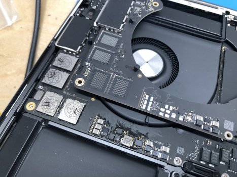
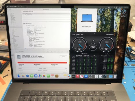
M3 Max 16” MacBook Pro upgrade from 512GB to 8TB SUCCESSFUL with 8x K5A8 NANDs after installing over 100 passive components (plus some voltage regulators)! Because there are no schematics available for this model, I referenced an M2 Pro 16” MacBook Pro schematic to painstakingly draw a set of diagrams to locate each of the necessary components on the M3 Max board (as all the components are identical between the two, the locations on the board, though, are not). I should note that I only installed the necessary components, and omitted a number of decoupling capacitors, which has proven to not be an issue. Installing those would bring the component total to almost 200... Which is a lot to solder by hand.
Relevant Mouser projects and parts:

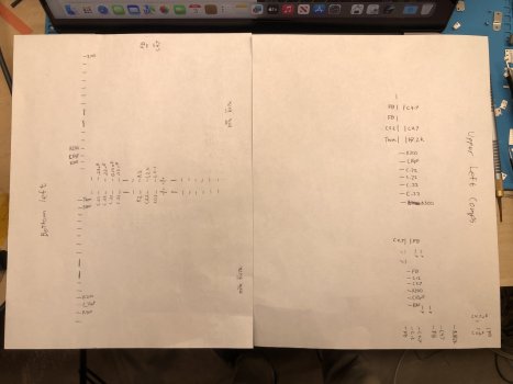
Relevant Mouser projects and parts:
- Mac NAND LP, one project order needed per added NAND: https://www.mouser.com/ProjectManager/ProjectDetail.aspx?AccessID=fd9bd9decb
- Mac NAND Power, all components needed to populate NAND1 power circuit on M2 and later, minus voltage regulator ICs: https://www.mouser.com/ProjectManager/ProjectDetail.aspx?AccessID=5633742c1f
- Mac NAND SSD1 Additions, some additional support components for second set of NANDs: https://www.mouser.com/ProjectManager/ProjectDetail.aspx?AccessID=0abaa47822
- 338S00600 voltage regulator: https://www.aliexpress.us/item/3256806668172757.html
- LT8642EV-1 voltage regulator: https://www.aliexpress.us/item/3256805855879468.html


If you can figure out which pin of the NAND it's connected to, I can tell you from a schematic. Otherwise I can measure mine.Hi, im doing a Mac Mini M4 Nand upgrade and accidentally destroyed this resistor. Does anybody know the value of this resistor(its in the side of the board that has a lot of IC). Thanks!
I'm trying to decipher some of the previous messages about M4 Pro (14" in particular) upgrade paths. It seems to be implied that a 4 package configuration (512 GB, 1 TB, 2 TB) can be upgraded as far as 4 TB with just 4 packages, but 8 TB requires all 8 packages populated. Is this correct? (I understand that on previous generations, 4 TB always required 8 packages.)
I have borrowed a friend’s mac mini and measured it. Its 47k ohm resistor. But after placing a new resistor, its still wont restore. Tried puting back the original nand and it still wont boot/restore. I guess i somehow destroyed the board… i tried measuring in continuity mode for the “gold pin” and they all show the same value as a normal module. I think my only hope is for when someone starts selling the module itself🥲If you can figure out which pin of the NAND it's connected to, I can tell you from a schematic. Otherwise I can measure mine.
No, on any machine with support for 8 NANDs, all 8 are required for both 8TB AND 4TB... 4x1TB NANDs is not a valid config on those models. Only the machines with support for only 4 NANDs (M3 Pro and presumably M4 Pro) support 4TB by way of 4x1TB NANDs.I'm trying to decipher some of the previous messages about M4 Pro (14" in particular) upgrade paths. It seems to be implied that a 4 package configuration (512 GB, 1 TB, 2 TB) can be upgraded as far as 4 TB with just 4 packages, but 8 TB requires all 8 packages populated. Is this correct? (I understand that on previous generations, 4 TB always required 8 packages.)
Your last sentence there was what I was trying to figure out. Can M4 Pro with 4 NANDs support 4 TB?No, on any machine with support for 8 NANDs, all 8 are required for both 8TB AND 4TB... 4x1TB NANDs is not a valid config on those models. Only the machines with support for only 4 NANDs (M3 Pro and presumably M4 Pro) support 4TB by way of 4x1TB NANDs.
From my previous conversation with him, what I understood was... Base (1tb) goes max to 2 TB...because they use 4x population scheme... as in.... for 1tb they use garbage 4x 256gb nands... and for 2tb they use 4x 512gb ..Your last sentence there was what I was trying to figure out. Can M4 Pro with 4 NANDs support 4 TB?
So if you'd put 4x 1TB nands in, the recovery DFU mode flash would not work, because the config for it understands that for the 4TB and 8TB versions you need 8x NANDs populated....instead of the provided 4x populated spaces... so inherently... a mis-match in config.
Presumably yes, as I believe it only has support for 4 NANDs like M3 Pro, though haven’t gotten to try it myself with M4 Pro. It should work with 4x K6B2 NANDs.Your last sentence there was what I was trying to figure out. Can M4 Pro with 4 NANDs support 4 TB?
This individual's purchaser review showed that the T-5 connection from the Mac is good but that the actual sustained speed of the OWC Ultra T-5 drive operates at T-3 speeds. I reckon the makers of externals have some way to go to achieve the claimed 6000 MB/s capability.
yes, there is a few videos on YouTube show this exact config getting a 4tb upgrade with just 4 nandsYour last sentence there was what I was trying to figure out. Can M4 Pro with 4 NANDs support 4 TB?
do we know the layout of the nand landing pads for the Mac mini m4 pro. I hear they support 8tb.... but do they really have 8 landing pads on that tiny thin removable storage board? if they have 8 then it is business as usual in terms of upgrading...
however I hear rumors this is the 1st Mac that uses 2tb nands(x4 for 8tb config).... I did not know 2tb nands of this size/spec had ever been used by apple. can anyone shed some light and maybe share an image of what the m4 pro landing pad layout is looking like?
much appreciated!
@gilles_polysoft @dosdude1
Yes, there is a new "K6B3" model 2TB NAND chip that they use. These are not yet available I don't think, so will be a bit until 8TB is doable on that model.do we know the layout of the nand landing pads for the Mac mini m4 pro. I hear they support 8tb.... but do they really have 8 landing pads on that tiny thin removable storage board? if they have 8 then it is business as usual in terms of upgrading...
however I hear rumors this is the 1st Mac that uses 2tb nands(x4 for 8tb config).... I did not know 2tb nands of this size/spec had ever been used by apple. can anyone shed some light and maybe share an image of what the m4 pro landing pad layout is looking like?
much appreciated!
@gilles_polysoft @dosdude1
Hello everyone, I’ve been searching for this thread for a long time, and I hope someone here can help me.
I decided to take a bold step and upgrade the memory on my 11-inch iPad Pro M1 (A2459).
I watched several videos where Chinese technicians carefully remove the old memory, install new chips, and happily enjoy having 2TB of storage instead of 128GB. Inspired, I decided to try the same. I ordered a set of two chips (H23B8T85K7AFJ-BC 136A) from AliExpress (the seller chose these chips for my iPad Pro).
I found a technician who had successfully done this kind of upgrade on iPhones, although he had never worked on iPads before. Fully aware of the risks, I decided to go through with the operation. However, I ran into a problem. When trying to load the firmware, I encountered error 4014.
I then tried leaving only one chip, but the same issue occurred. I experimented with different combinations, but the outcome was always error 4014 or error 9.
I came to the conclusion that the issue lies in powering the memory chip. Most likely, the 1TB module requires more power to boot, or the correct configuration of resistors in specific locations is necessary to make this memory modules work properly.
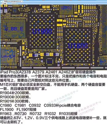
The sellers sent me an image, but the diagram that the seller provided me is of very poor quality and it is not clear where these resistors should be placed/changed. I started digging online and purchased schematics, but they didn’t include a diagram of the motherboard.
I’ve scoured the internet but haven’t been able to find schematics that clearly show how to position the resistors to make the memory work.
Could you please help me figure this out? Does anyone have high-resolution photos of the motherboard with 2TB memory?
Thanks in advance to everyone
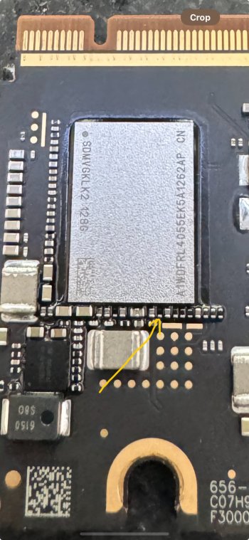
P.S.:in the picture the model index is from a 13 inch tablet with the same processor. they should be identical to mine
Attachments
Did you verify the chips were blank before installing them? This is very important unless the chips you got were sold as being pre-programmed (in which case they will be labeled 0 and 1). Also, if your device came with only one NAND installed, then you will also have to add the necessary ~30 passive components (resistors, capacitors, etc) to allow use of the second NAND. If you tried to restore without these, the NAND in position 0 has now likely been programmed improperly, and you’ll need to install a new blank set of NANDs.Hello everyone, I’ve been searching for this thread for a long time, and I hope someone here can help me.
I decided to take a bold step and upgrade the memory on my 11-inch iPad Pro M1 (A2459).
I watched several videos where Chinese technicians carefully remove the old memory, install new chips, and happily enjoy having 2TB of storage instead of 128GB. Inspired, I decided to try the same. I ordered a set of two chips (H23B8T85K7AFJ-BC 136A) from AliExpress (the seller chose these chips for my iPad Pro).
I found a technician who had successfully done this kind of upgrade on iPhones, although he had never worked on iPads before. Fully aware of the risks, I decided to go through with the operation. However, I ran into a problem. When trying to load the firmware, I encountered error 4014.
I then tried leaving only one chip, but the same issue occurred. I experimented with different combinations, but the outcome was always error 4014 or error 9.
I came to the conclusion that the issue lies in powering the memory chip. Most likely, the 1TB module requires more power to boot, or the correct configuration of resistors in specific locations is necessary to make this memory modules work properly.
The sellers sent me an image, but the diagram that the seller provided me is of very poor quality and it is not clear where these resistors should be placed/changed. I started digging online and purchased schematics, but they didn’t include a diagram of the motherboard.
I’ve scoured the internet but haven’t been able to find schematics that clearly show how to position the resistors to make the memory work.
Could you please help me figure this out? Does anyone have high-resolution photos of the motherboard with 2TB memory?
Thanks in advance to everyone
P.S.:in the picture the model index is from a 13 inch tablet with the same processor. they should be identical to mine
they were blank. seller saidDid you verify the chips were blank before installing them? This is very important unless the chips you got were sold as being pre-programmed (in which case they will be labeled 0 and 1).
after installing only one memory chip, the error still popped up 4014. that's why I decided that it should be possible for a 1 TB chip to have a different arrangement of passive componentsAlso, if your device came with only one NAND installed, then you will also have to add the necessary ~30 passive components (resistors, capacitors, etc) to allow use of the second NAND. If you tried to restore without these, the NAND in position 0 has now likely been programmed improperly, and you’ll need to install a new blank set of NANDs.
this is brilliant work... have you made a video on this??M3 Max 16” MacBook Pro upgrade from 512GB to 8TB SUCCESSFUL with 8x K5A8 NANDs after installing over 100 passive components (plus some voltage regulators)! Because there are no schematics available for this model, I referenced an M2 Pro 16” MacBook Pro schematic to painstakingly draw a set of diagrams to locate each of the necessary components on the M3 Max board (as all the components are identical between the two, the locations on the board, though, are not). I should note that I only installed the necessary components, and omitted a number of decoupling capacitors, which has proven to not be an issue. Installing those would bring the component total to almost 200... Which is a lot to solder by hand.
Relevant Mouser projects and parts:
- Mac NAND LP, one project order needed per added NAND: https://www.mouser.com/ProjectManager/ProjectDetail.aspx?AccessID=fd9bd9decb
- Mac NAND Power, all components needed to populate NAND1 power circuit on M2 and later, minus voltage regulator ICs: https://www.mouser.com/ProjectManager/ProjectDetail.aspx?AccessID=5633742c1f
- Mac NAND SSD1 Additions, some additional support components for second set of NANDs: https://www.mouser.com/ProjectManager/ProjectDetail.aspx?AccessID=0abaa47822
- 338S00600 voltage regulator: https://www.aliexpress.us/item/3256806668172757.html
- LT8642EV-1 voltage regulator: https://www.aliexpress.us/item/3256805855879468.html
View attachment 2458598View attachment 2458599View attachment 2458600View attachment 2458601
1x 1TB is not a valid config, so that will never work. If you tried to restore that way, that chip has been improperly programmed and now can no longer be used.after installing only one memory chip, the error still popped up 4014. that's why I decided that it should be possible for a 1 TB chip to have a different arrangement of passive components
@
also is it the port next to the MagSafe charger you are using to restore when connecting to the host Mac machine?
@dosdude1 in this you mentioned you didn't have the exact schematic.... could you please share the one that you have been referring to while performing the upgrade? the m2 pro 16inch pleaseM3 Max 16” MacBook Pro upgrade from 512GB to 8TB SUCCESSFUL with 8x K5A8 NANDs after installing over 100 passive components (plus some voltage regulators)! Because there are no schematics available for this model, I referenced an M2 Pro 16” MacBook Pro schematic to painstakingly draw a set of diagrams to locate each of the necessary components on the M3 Max board (as all the components are identical between the two, the locations on the board, though, are not). I should note that I only installed the necessary components, and omitted a number of decoupling capacitors, which has proven to not be an issue. Installing those would bring the component total to almost 200... Which is a lot to solder by hand.
Relevant Mouser projects and parts:
- Mac NAND LP, one project order needed per added NAND: https://www.mouser.com/ProjectManager/ProjectDetail.aspx?AccessID=fd9bd9decb
- Mac NAND Power, all components needed to populate NAND1 power circuit on M2 and later, minus voltage regulator ICs: https://www.mouser.com/ProjectManager/ProjectDetail.aspx?AccessID=5633742c1f
- Mac NAND SSD1 Additions, some additional support components for second set of NANDs: https://www.mouser.com/ProjectManager/ProjectDetail.aspx?AccessID=0abaa47822
- 338S00600 voltage regulator: https://www.aliexpress.us/item/3256806668172757.html
- LT8642EV-1 voltage regulator: https://www.aliexpress.us/item/3256805855879468.html
View attachment 2458598View attachment 2458599View attachment 2458600View attachment 2458601
also is it the port next to the MagSafe charger you are using to restore when connecting to the host Mac machine?
Last edited:
Here you go. You need to stuff BOM options "SSD_OC1VR1" and "SSD_8L" to use all 8 NANDs. Yes, USB-C port closest to the MagSafe port is the port used for DFU restore.@
@dosdude1 in this you mentioned you didn't have the exact schematic.... could you please share the one that you have been referring to while performing the upgrade? the m2 pro 16inch please
also is it the port next to the MagSafe charger you are using to restore when connecting to the host Mac machine?
Attachments
Thank you very much!Here you go. You need to stuff BOM options "SSD_OC1VR1" and "SSD_8L" to use all 8 NANDs. Yes, USB-C port closest to the MagSafe port is the port used for DFU restore.
... apologies for dumb questions but:
ive been using board view with no issue as most of the files im opening are in*.bvr file format. however this one is in a *.cad file format. my MacBook (m1pro) is struggling to read this using 'openboardview' from GitHub. most of the places ive read up on said it should be able to read it since the 2022 update but im having no joy.
any info would be appreciated. thanks
Register on MacRumors! This sidebar will go away, and you'll see fewer ads.


