Apple's been in the custom silicon game for over a decade, and the Apple Silicon Mac releases are just the latest incarnations.
Heck, their
phones have custom NVMe controllers - and from all appearances it looks like Apple's been making preparations to leave Intel since they requested ARM put together ARMv8 and the 64 bit Instruction Set Architecture (AArch64) used in the A7 and the iPhone 5s released in 2013 (so planning would've had to have started around 2011).
Here's my standard blurb on the Apple Silicon Team for those unfamiliar with the evolution of Apple Silicon:
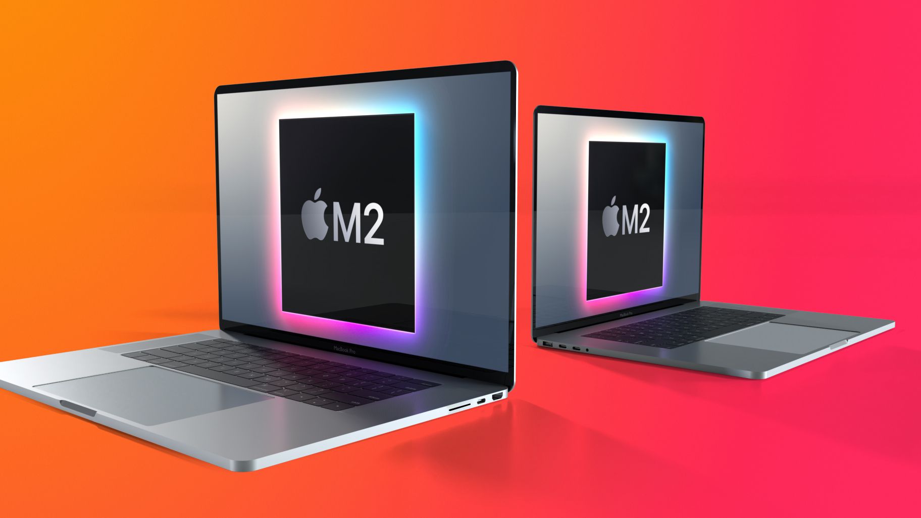
M1 has 4 high performance Firestorm and 4 high efficiency Icestorm cores - it was designed for the low-end MacBook Air (fanless) and 13" MacBook Pro models as part of their annual spec bump.
Rumor has it the M1x slated for release
real soon now will have 8 Firestorm cores (depending on binning) and 2 Icestorm cores and will be targeted at machines like the 14" and 16" MacBook Pros and possibly the high end Mac Mini.
In 2008, Apple acquired PA Semi and worked with cash strapped Intrinsity and Samsung to produce a FastCore Cortex-A8; the frenemies famously split and Apple used their IP and Imagination's PowerVR to create the A4 and Samsung took their tech to produce the Exynos 3. Apple acquired Intrinsity and continued to hire engineering talent from IBM's Cell and XCPU design teams, and hired Johny Srouji from IBM who worked on the POWER7 line to direct the effort.
This divergence from standard ARM designs was continued by Apple who continued to nurture and build their Silicon Design Team (capitalized out of respect) for a decade, ignoring standard ARM designs building their own architecture, improving and optimizing it year by year for the last decade.
Whereas other ARM processor makers like Qualcomm and Samsung pretty much now use standard ARM designed cores - Apple has their own designs and architecture and has greatly expanded their own processor acumen to the point where the Firestorm cores in the A14 and M1 are the most sophisticated processors in the world with an eight wide processor design with a 690 instruction execution queue with a massive reorder buffer and the arithmetic units to back it up - which means its out-of-order execution unit can execute up to eight instructions
simultaneously.
x86 processor makers are hampered by the CISC design and a variable instruction length. This means that at most they can produce a three or four wide design for an instruction subset, and even for that the decoder would have to be fiendishly clever, as it would have to guess where one instruction ended and the next began.
There's a problem shared with x86-64 processor makers and Windows - they never met an instruction or feature they didn't like. What happens then is you get a build-up of crud that no one uses, but it still consumes energy and engineering time to keep working.
AMD can get better single core speed by pushing up clocks (and dealing with the exponentially increased heat though chiplets are probably much harder to cool), and Intel by reducing the number of cores (the top of the 10 core 20 thread 10900K actually had to be shaved to achieve enough surface area to cool the chip so it at 14nm had reached the limits of physics). Both run so hot they are soon in danger of running into Moore's Wall.
Apple OTOH ruthlessly pares underused or unoptimizable features.
When Apple determined that ARMv7 (32 bit ARM) was unoptimizable, they wrote it out of iOS, and removed those logic blocks from their CPUs in
two years, repurposing the silicon real estate for more productive things. Intel, AMD, and yes even Qualcomm couldn't do that in a
decade.
Apple continues that with
everything - not enough people using Force Touch - deprecate it, remove it from the hardware, and replace it with Haptic Touch. Gone.
Here's another secret of efficiency - make it a goal. Two years ago on the A13 Bionic used in the iPhone 11s, the Apple Silicon Team introduced hundreds of voltage domains so they could turn off parts of the chip not in use. Following their annual cadence, they increased the speed of the Lightning high performance and the Thunder high efficiency cores by 20% despite no change in the 7nm mask size. As an aside, they increased the speed of matrix multiplication and division by six times (used in machine learning).
Last year they increased the speed of the Firestorm high performance and Icestorm high efficiency cores by another 20% while dropping the mask size from 7nm to 5nm. That's a hell of a compounding rate and explains how they got to where they are. Rumor has it they've bought all the 3nm capacity from TSMC for the A16 (and probably M3) next year.
Wintel fans would deny the efficacy of the A series processors and say they were mobile chips, as if they used slower silicon with wheels on the bottom or more sluggish electrons.
What they
were were
high efficiency chips which were passively cooled and living in a glass sandwich. Remove them from that environment where they could breathe more easily and boost the clocks a tad and they became a raging beast.
People say that the other processor makers will catch up in a couple of years, but that's
really tough to see. Apple Silicon is the culmination of a decade of intense processor design financed by a company with
very deep pockets - who is fully cognizant of the competitive advantage Apple Silicon affords. Here's an article in Anandtech comparing the Firestorm cores to the competing ARM and x86 cores. It's very readable for an article of its ilk:
Seeking answers? Join the AnandTech community: where nearly half-a-million members share solutions and discuss the latest tech.

www.anandtech.com
Of course these are the Firestorm cores used in the A14, and are not as performant as the cores in the M1 due to the M1's higher 3.2 ghz clock speed.


